Advanced Materials for Electronics Market Report Scope and Overview:
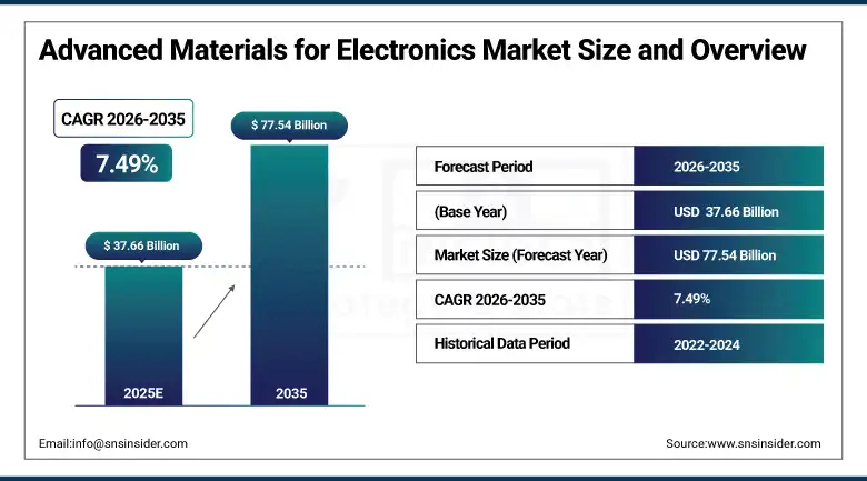
The Advanced Materials for Electronics Market size was valued at USD 37.66 Billion in 2025E and is projected to reach USD 77.54 Billion by 2035, at 7.49% CAGR from 2026-2035.
Demand for SiC, GaN, graphene, and nanomaterials in EVs, 5G, IoT, and flexible devices has been driving the boom for the advanced materials for electronics market trends. Furthermore, trends related to sustainability and miniaturization drive innovation on composite materials, printable electronics, and biodegradable materials.
High-speed computing and growing AI penetration in next-gen devices has spurred demand for high-performance electronics, which is driving the expansion of the advanced materials for electronics market growth. R&D spending is expanding, backed by governmental policies promoting semiconductor manufacturing and evolving innovation. Improved Conductivity, flexibility, and durability of these materials are facilitating the development of next-generation sensors, wearable electronics, and quantum devices. Furthermore, the movement in favor of edge computing and miniaturized circuits is generating high application demand for specialty materials suitable for power-dense low-EMI electronics.
By the end of 2024, global 5G connections reached 2.25 billion, marking a substantial leap in adoption and enabling real-time data processing capabilities essential for Advanced Materials for Electronics.
Advanced Materials for Electronics Market Size and Growth:
-
Market Size in 2025E: USD 37.66 Billion
-
Market Size by 2035: USD 77.54 Billion
-
CAGR: 7.49% from 2026 to 2035
-
Base Year: 2025E
-
Forecast Period: 2026–2035
-
Historical Data: 2022–2024
To Get More Information On Advanced Materials for Electronics Market - Request Free Sample Report
Advanced Materials for Electronics Market Highlights:
-
The U.S. government, through the CHIPS Program Office, has allocated multi-billion-dollar federal incentives to major semiconductor fabrication projects, significantly increasing demand for advanced electronic materials used in next-generation chip manufacturing.
-
India’s Electronics System Design and Manufacturing sector is projected to expand rapidly, supported by national policies targeting a USD 400 billion domestic manufacturing output, thereby strengthening local consumption of advanced electronic materials.
-
Government-backed Production-Linked Incentive schemes in India have generated over INR 8,390 crore in new investments for electronics manufacturing, directly stimulating demand for high-performance and specialty materials.
-
U.S. export controls on advanced computing and semiconductor manufacturing technologies are reshaping global supply chains, emphasizing the strategic importance of advanced materials in high-technology electronics.
-
National policies promoting electric vehicles, 5G infrastructure deployment, and artificial intelligence hardware are accelerating electronics production, indirectly driving sustained demand for advanced materials across multiple applications.
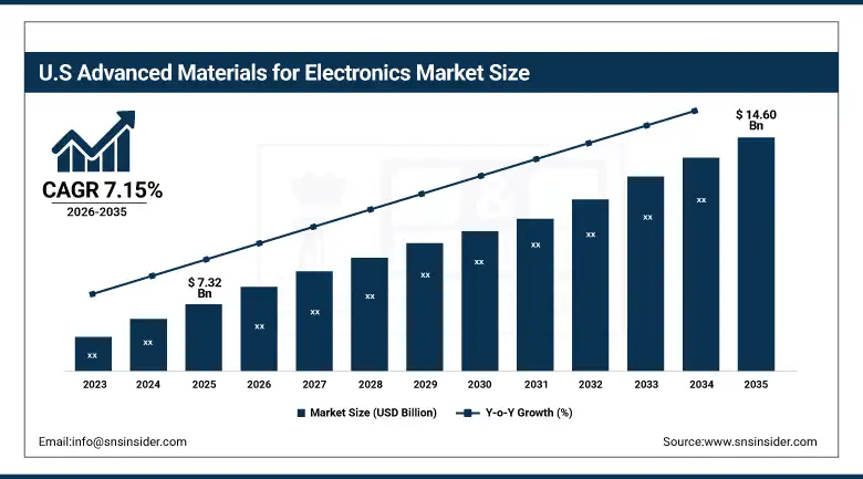
U.S. Advanced Materials for Electronics Market Size Outlook
The U.S. Advanced Materials for Electronics Market size is estimated to be valued at USD 7.32 billion in 2025E and is projected to grow at a CAGR of 7.15%, reaching USD 14.60 billion by 2035. Developments in the U.S. growth factors supporting advanced materials for electronics accelerated CHIPS Act funding, government incentives for strategic domestic production of critical minerals, increasing demand for advanced materials due to 5G, EVs, AI and data centers and growing semiconductor R&D under federal support and funding.
Advanced Materials for Electronics Market Drivers:
-
Rising Demand for Advanced Materials Driven by AI 5G EVs and Next Generation Semiconductors
Demand for low-K dielectrics and high-purity silicon is strong on continued global adoption of miniaturization, high-performance semiconductors for AI, 5G, IoT, and edge computing. Interests in wide bandgap semiconductors (SiC and GaN) for power electronics and grid updates are fostered by the increasing Electric Vehicle and renewable energy sectors. At the same time increasing efforts to innovate in materials using AI, machine learning and high-throughput discovery are shortening development cycles for next-gen composites, nanomaterials and smart polymers.
-
In 2024, TSMC announced a USD 25 billion investment into advanced chip production focused on AI and edge computing, significantly boosting demand for low-K dielectrics and high-purity silicon wafers.
Advanced Materials for Electronics Market Restraints:
-
Scalability Issues and Resource Dependency Challenge Growth of Advanced Materials in Emerging Electronics Sector
The presence of limited or non-scalable and reproducible nature of materials, such as 2D materials (graphene and MXenes) and novel dielectrics, employed in emerging electronics can hinder the growth of the advanced materials for electronics market. The attractive properties of these materials are often poorly realized in practice, however, due to production challenges that yield samples with considerable quality variation, delaying their commercial adoption. Supply chains over-reliance on rare or geopolitically sensitive elements including indium, gallium and rare earths cause challenges for secure and reliable access in the long term, especially during escalation in geopolitical tensions.
Advanced Materials for Electronics Market Opportunities:
-
Sustainable Materials and Regional Growth Drive New Opportunities in Advanced Electronics Manufacturing Worldwide
The shift toward sustainable and eco-friendly materials such as biodegradable photoresists, green solvents, and extensively recycled substrates opens new market avenues in electronics manufacturing. There’s also a significant opportunity in specialty materials for advanced semiconductor fabs, including EUV photoresists, 2D materials (graphene and MXenes), and reticular frameworks tailored for flexible sensors and photonics. Furthermore, emerging markets particularly in Asia-Pacific, Latin America, and Africa are growing electronics manufacturing hubs where localized supply of high-performance materials can reduce costs and support regional technology ecosystems.
-
Saudi Arabia and UAE installed high-frequency laminates for 5G, with Egypt funding a USD 300 million semiconductor-AI fund in 2024 and nurturing 23 startups, including a USD 10 million seed for InfiniLink.
Advanced Materials for Electronics Market Segment Analysis:
By Type
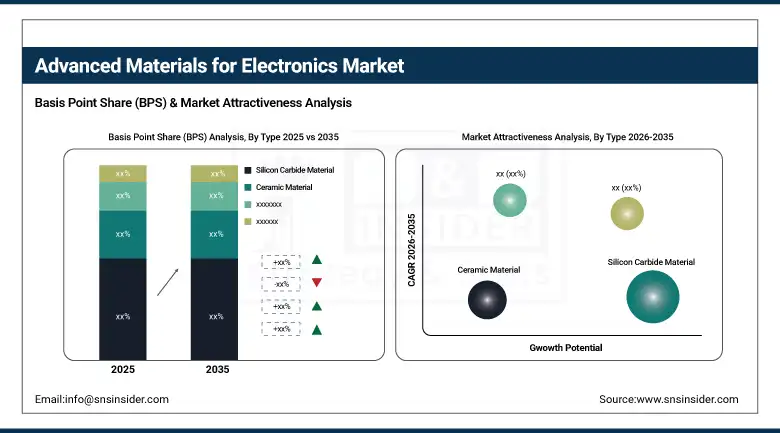
In 2025E, Silicon Carbide (SiC) material held a dominant advanced materials for electronics market share, accounting for a 32.4% due to its superior performance in high-power and high-temperature applications. SiC is widely used in electric vehicle inverters, fast-charging infrastructure, industrial motor drives, and renewable energy systems. Its ability to reduce energy losses, improve thermal conductivity, and enhance switching efficiency has made it a preferred material in power electronics. Major players, such as STMicroelectronics, Infineon, and Wolfspeed expanded their SiC production capacities to meet growing demand, further solidifying its dominant position.
Graphene is expected to be the fastest-growing material during the forecast period over 2026-2035 as it has superior electrical, thermal, and mechanical properties. This material is getting more advanced consideration for next-generation flexible electronics, sensors, photonics and advanced transistors. As more and more research continues on the material, combined with the steadily cheaper manufacturing process and its potential revolutionary use in energy storage and in wearables, graphene is set to transform the way consumer electronics will be produced in the next few years.
By Application
In 2025E, the advanced materials for electronics market for semiconductor accounted for 28.6% share, in line with growing demand for high performance chips commonly used in AI, data center, 5G and automotive applications. With miniaturization, energy efficiency and speed being the need of the hour, various advanced materials, such as low-K dielectrics, silicon carbide and gallium nitride have found adoption in semiconductor manufacturing. Semiconductors are the largest, and will remain the largest market segment, with advanced foundries and integrated device manufacturers (IDMs) continuing to expand the use of enhancive materials to enhances chip performance, reliability and thermal management.
Over 2026-2035, the fastest growth in the global wearable electronic devices market is expected to be driven by developments in health management, fitness monitoring, and consumer electronics. Although, increasing utilization of flexible, lightweight, and biocompatible materials has unlocked the pathways of smart textiles, e-skin and next-gen wearables. The continual improvement of new technology, such as printable electronics, stretchable substrate, and self-healing materials are all anticipated to further accelerate growth in this dynamic market segment.
Advanced Materials for Electronics Market Regional Analysis:
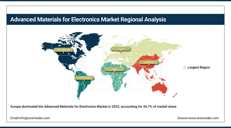
Europe Advanced Materials for Electronics Market Trends:
The advanced materials for electronics market in Europe accounted for 34.7% in 2025E, supported by high investments in semiconductor research and development, favorable regulations focused on sustainability in electronics, and an elaborated semiconductor manufacturing ecosystem in the region. A combination of green energy transition priorities and a transition in transportation to electrification has intensified the usage of materials including silicon carbide and GaN in power devices. Moreover, research partnerships between academia and industry are also enabling innovations on 2D materials, bioelectronics, and green substrates. Regional capabilities have been bolstered by supportive policies, including those promoting clean technology, digital transformation, and local supply chains.
European demand for advanced electronic materials was led by Germany, driven by the country's leadership in power semiconductors, RF components, and industrial sensor materials. Regional R&D infrastructure with support policies, ongoing EU semiconductor initiatives, and cooperation between industry and academia are driving innovation in compound semiconductors, high‑performance substrates, and sustainable materials.
Get Customized Report as Per Your Business Requirement - Enquiry Now
Asia-Pacific Advanced Materials for Electronics Market Trends:
Asia Pacific is expected to be the fastest-growing region in the advanced materials for electronics market over 2026-2035 due to the rapid industrialization and rise in electronics manufacturing capacity coupled with a growing consumer electronics, EVs, and smart devices market in the region. Well-established availability of raw materials, skilled labor, and capital investments in semiconductor fabrication and materials R&D are advantages for the region, coupled with increasing use of advanced materials (for GaNs, SiCs, and 2Ds), driven by the booming adoption of flexible electronics, IoT devices, and high-frequency communication technologies in the region. This trend is boosting market potential from development and government initiatives toward digitalization and renewable energy from different electronics applications only adds to effort.
China accounted for the largest share of the demand for advanced materials in Asia Pacific, owing to huge electronics manufacturing and critical-materials processing in the country.
North America Advanced Materials for Electronics Market Trends:
North America is expected to be a significant region for advanced materials for electronics, where demand is underpinned by innovation ecosystems, new investments in semiconductor fabrication, and emerging demand for next-generation electronics. In the region, advanced materials are being increasingly adopted in AI chips, aerospace electronics, electric vehicles, and quantum computing, among others. Strong links between research institutes and industry are speeding progress on nanomaterials, photonic materials, and sustainable electronics. Moreover, supportive policies for chip manufacturing reshoring are increasing regional autonomy and the evolution of material supply chains.
The U.S. continued to lead North America in advanced electronic materials demand, thanks to ramped-up domestic chip fabs (particularly in Arizona and Texas), tens of billions in CHIPS Act funds, and increasing high‑purity materials consumption.
Latin America and Middle East & Africa Advanced Materials for Electronics Market Trends:
Advanced materials for electronics market in Latin America and the Middle East & Africa (MEA) are expected to develop with a promising rate during the forecast period. Rising investment in electronics manufacturing, renewable energy, and digital infrastructure underpins the growth. The two regions are known for honing efforts in building regional semiconductor industries and manufacturing smart devices. New flexible materials, advanced substrates and power electronics are the focus of several different innovation initiatives backed by government and foreign partnerships. These regions are turning into strategic hubs for sourcing materials and developing applications, driven by demand for smart technologies and energy-efficient solutions.
Advanced Materials for Electronics Market Competitive Landscape:
ASML Holding N.V. is a global leader Established in 1984, in advanced semiconductor manufacturing equipment. Headquartered in the Netherlands, the company specializes in lithography systems, including EUV technology, enabling production of cutting-edge integrated circuits for logic and memory chipmakers worldwide.
-
In June 2024, ASML and imec opened a High Numerical Aperture (NA) EUV lithography lab in Veldhoven, providing access to prototype EUV systems and developing advanced resist materials paving the way for sub‑20 nm patterning.
DuPont de Nemours, Inc. is a global science and innovation company Established in 1802 delivering advanced materials and solutions. It serves electronics, water, protection, and industrial markets, focusing on semiconductors, sustainable materials, and high-performance technologies for diverse end-use industries worldwide.
-
In February 2025, DuPont announced further enhancements on sustainable EUV resist chemistry (including KrF UV resists) at the SPIE Advanced Lithography + Patterning conference.
Advanced Materials for Electronics Companies are:
-
Shin-Etsu Chemical Co., Ltd.
-
Soitec SA
-
NXP Semiconductors N.V.
-
NAURA Technology Group Co., Ltd.
-
BASF SE
-
3M Company
-
Samsung SDI Co., Ltd.
-
Hitachi Chemical Co., Ltd. (Resonac Holdings)
-
Sumitomo Chemical Co., Ltd.
-
Tokyo Ohka Kogyo Co., Ltd.
-
JSR Corporation
-
Merck KGaA (EMD Electronics)
-
LG Chem Ltd.
-
Mitsubishi Chemical Group Corporation
-
Applied Materials, Inc.
-
Lam Research Corporation
-
SK Materials Co., Ltd.
-
Intel Corporation
| Report Attributes | Details |
|---|---|
| Market Size in 2025E | USD 37.66 Billion |
| Market Size by 2035 | USD 77.54 Billion |
| CAGR | CAGR of 7.49% From 2026 to 2035 |
| Base Year | 2025E |
| Forecast Period | 2026-2035 |
| Historical Data | 2022-2024 |
| Report Scope & Coverage | Market Size, Segments Analysis, Competitive Landscape, Regional Analysis, DROC & SWOT Analysis, Forecast Outlook |
| Key Segments | • By Type (Graphene Material, Silicon Carbide Material, Ceramic Material, Smart Glass Material, and Others) • By Application (Photovoltaic Cells, Displays, Touch Screens, Sensors, Semiconductors, Wearable Electronics Devices, Biomedical Devices, and Others) |
| Regional Analysis/Coverage | North America (US, Canada), Europe (Germany, UK, France, Italy, Spain, Russia, Poland, Rest of Europe), Asia Pacific (China, India, Japan, South Korea, Australia, ASEAN Countries, Rest of Asia Pacific), Middle East & Africa (UAE, Saudi Arabia, Qatar, South Africa, Rest of Middle East & Africa), Latin America (Brazil, Argentina, Mexico, Colombia, Rest of Latin America). |
| Company Profiles | Some of the major Advanced Materials for Electronics market players include ASML Holding NV, Shin-Etsu Chemical Co., Ltd., Soitec SA, NXP Semiconductors N.V., NAURA Technology Group, BASF SE, DuPont de Nemours, 3M Company, Samsung SDI, Hitachi Chemical (Resonac), Sumitomo Chemical, Tokyo Ohka Kogyo, JSR Corporation, Merck KGaA, LG Chem, Mitsubishi Chemical Group, Applied Materials, Lam Research, SK Materials, and Intel Corporation. |
Frequently Asked Questions
Ans: Europe dominated the Advanced Materials for Electronics Market in 2025.
Ans: The Silicon Carbide Material segment dominated the Advanced Materials for Electronics Market in 2025.
Ans: The major growth factor of the Advanced Materials for Electronics Market is the rising demand for miniaturized, high-performance semiconductors driven by AI, 5G, IoT, electric vehicles, and advanced computing applications.
The Advanced Materials for Electronics Market size was valued at USD 37.66 Billion in 2025E and is projected to reach USD 77.54 Billion by 2035, at 7.49% CAGR from 2026-2035.
Ans: The Advanced Materials for Electronics Market is expected to grow at a CAGR of 7.49% from 2026-2035.
Get in Touch
