Copper Pillar Bump (CPB) Market Size Analysis:
The Copper Pillar Bump (CPB) Market Size was valued at USD 1.85 billion in 2025 and is expected to grow at 8.32% CAGR to reach USD 4.11 billion by 2035.
The global Copper Pillar Bump (CPB) Market is experiencing robust growth, fueled by the increasing demand for fine pitch interconnects and advanced semiconductor packaging. Vivid momentum is offered by boosting 5G penetration, fast miniaturization of electronics and increasing complexity in electronic products. The market is gaining advantages of increasing use in consumer electronics, automotive, and industrial applications. With chip design innovation and the need for high-performance/ reliable interconnects driving next-generation semiconductor fabrication, CPB is emerging as a technology of choice, providing scalability, lower thermal, and superior electrical performance.
Market Size and Forecast: 2025
-
Market Size in 2025 USD 1.85 Billion
-
Market Size by 2035 USD 4.11 Billion
-
CAGR of 8.32% From 2026 to 2035
-
Base Year 2025
-
Forecast Period 2026-2035
-
Historical Data 2022-2024

To Get more information on Copper Pillar Bump (CPB) Market - Request Free Sample Report
Copper Pillar Bump (CPB) Market Trends:
-
Growing adoption of advanced chip packaging technologies in high-performance computing, cloud infrastructure, and hyperscale data centers.
-
Increasing use of copper pillar bump interconnects to support higher power efficiency, improved signal integrity, and thermal performance.
-
Rising demand for multi-die and compact semiconductor architectures driven by AI, big data analytics, and real-time processing workloads.
-
Expanding application of CPB technology in electric and autonomous vehicles, supporting high-density and high-reliability automotive electronics.
-
Increasing semiconductor content per vehicle, boosting demand for robust interconnect solutions in advanced driver assistance and autonomous driving systems.
The U.S. Copper Pillar Bump (CPB) Market size was USD 0.31 billion in 2025 and is expected to reach USD 0.76 billion by 2035, growing at a CAGR of 9.25% over the forecast period of 2026–2035. The US copper pillar bump (CPB) market growth is mainly attributed to the increasing requirement for high-end packaging of semiconductors in the consumer electronics and automotive applications. Rising utilization of miniaturized and improved electronic devices, combined with large investments for domestic semiconductor production in line with U.S. government programs is driving the market growth.
According to research, as of 2024, more than 20 new semiconductor fabs are under development across the U.S., boosting demand for local advanced packaging solutions like CPB.

Copper Pillar Bump (CPB) Market Growth Drivers:
-
Rising need for advanced packaging in high-performance computing and data centers drives CPB adoption across enterprise semiconductor applications.
The rising implementation of advanced chip packaging in HPC systems, cloud infrastructure, and hyperscale data centers is driving the demand for the latest chip packaging technologies. The bump’s power performance, resistance and signal integrity is optimized for newer enterprise computing CPUs, GPUs and memory modules. With the expanding use of artificial intelligence, big data analytics and real-time processing, CPBs allow in-demand compact systems with high-speed, multi-die. Customer requirement This increasing performance need in data-driven markets is driving strong demand for CPB-based interconnect solutions in enterprise and industrial semiconductor applications.
According to research, over 90% of flagship smartphones in 2024 used processors packaged with CPB technology, ensuring faster processing and thermal efficiency.
Copper Pillar Bump (CPB) Market Restraints:
-
Thermal management and reliability issues in fine-pitch CPB interconnects pose challenges in high-performance applications.
Due to the continual decrease in chip architectures, the pitch size of CPBs decreases as well, with the result that during operation, these fractions possibly raises new thermal and mechanical stress problems. Fine-pitch CPBs are prone to warping, cracking, and thermal-fatigue, and this effect is more pronounced in harsh or challenging environments, such as automotive or aerospace application, which experience a wide range of temperature variation and vibration conditions. Providing long-term reliability under continuous thermal cycling and high current loads becomes more challenging as the underfill materials that are more and more robust involved, the design is optimized, the simulation tools become more advanced, and the quality test is stricter. Such reliability concerns serve as a major barrier to adoption of CPB in mission-critical or harsh environment applications.
Copper Pillar Bump (CPB) Market Opportunities:
-
Surging demand for advanced packaging in electric vehicles and autonomous driving systems unlocks new growth avenues.
Electric and autonomous vehicles rely heavily on complex sensor arrays, radar systems, high-speed processors, and real-time connectivity, all of which demand high-reliability, high-density chip packaging. Copper Pillar Bumps are well-suited to meet these requirements due to their superior electrical performance and mechanical stability. As EV manufacturers increase investments in smart systems and semiconductor content per vehicle rises, CPB technology stands to gain significant traction as a go-to solution for robust and compact interconnect architectures in automotive electronics.
According to research, an autonomous car may include 8–12 cameras, each feeding high-throughput data to processors that benefit from copper pillar interconnects for speed and thermal control.
Copper Pillar Bump (CPB) Market Segment Analysis:
By Bumping Technology
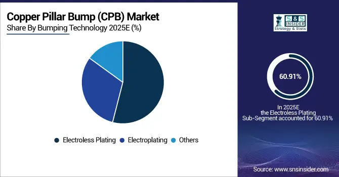
The Electroless Plating segment dominated the Copper Pillar Bump (CPB) Market share of 60.91% in 2025, due to its superior uniformity, cost-effectiveness, and compatibility with high-density interconnect (HDI) substrates. It eliminates the need for external power sources, making it ideal for advanced semiconductor packaging. The process supports finer pitch capabilities and better thickness control, which are crucial for emerging microelectronics applications, thereby making it the preferred choice across various high-volume manufacturing processes. The Electroplating segment is expected to grow at the fastest CAGR of 9.87% from 2026 to 2035 due to its scalability, precision in deposition, and increasing demand in advanced IC packaging technologies. Copper Pillar Bump (CPB) Companies like Shinko Electric Industries Co., Ltd. are significantly investing in electroplating techniques to enhance package reliability and throughput. As semiconductor devices continue to shrink, the need for finer, uniform metal deposits becomes critical, particularly for power and RF applications where Shinko’s innovations are well-aligned.
By Application
The Consumer Electronics segment dominated the Copper Pillar Bump (CPB) Market in 2025 with a 33.79% revenue share due to the massive production volumes of smartphones, tablets, and wearable devices. The rising consumer demand for compact, high-performance, and energy-efficient electronics has significantly increased the use of CPB in device miniaturization and enhanced performance. For instance, TSMC supports major electronics brands by utilizing CPB in its advanced packaging services, enabling next-gen device capabilities at scale. The Automotive segment is projected to grow at the fastest CAGR of 9.72% from 2026 to 2035, driven by the increasing adoption of electric vehicles (EVs), advanced driver assistance systems (ADAS), and infotainment systems. These applications demand robust, thermally efficient, and reliable semiconductor interconnects. Amkor Technology, Inc. is a key player focusing on automotive-grade packaging solutions, using CPB technology to meet the stringent reliability and thermal performance standards required in modern vehicles.
By Type
The Cu Bar Type segment captured the largest market share at 36.24% in 2025, owing to its widespread use in applications requiring higher mechanical strength and thermal stability. Its excellent current carrying capacity and robust interconnection capability make it a popular choice for power devices and RF applications. ASE Group leverages Cu bar bumping in its system-in-package (SiP) services to enable high-performance and compact electronic systems for communication and computing. The Fine Pitch Cu Pillar segment is forecasted to grow at the highest CAGR of 9.87% between 2026 and 2035, propelled by the increasing miniaturization of semiconductor components and the demand for higher I/O density. Fine pitch solutions enable smaller bump sizes and tighter pitch spacing, which are essential for next-generation ICs. JCET Group is advancing its fine pitch bumping capabilities to support ultra-high-density and 3D packaging, critical for modern mobile and AI devices.
Copper Pillar Bump (CPB) Market Regional Analysis:
Asia Pacific Copper Pillar Bump (CPB) Market Insights
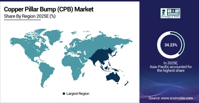
Asia Pacific dominated the Copper Pillar Bump (CPB) Market in 2025 with a 34.23% revenue share, primarily due to the region’s strong semiconductor manufacturing base, especially in countries like China, Taiwan, South Korea, and Japan. The high concentration of foundries, packaging houses, and OEMs, along with strong government support and investments in electronics manufacturing, contributes to the region's dominance. Additionally, the region’s leadership in consumer electronics production further boosts CPB adoption.
Get Customized Report as per Your Business Requirement - Enquiry Now
-
China leads the Asia Pacific CPB Market owing to its massive electronics manufacturing ecosystem, large-scale semiconductor production, and heavy investments in advanced packaging technologies. Strategic government initiatives and growing domestic demand for consumer electronics bolster its regional dominance.
North America Copper Pillar Bump (CPB) Market Insights
North America is expected to grow at the fastest CAGR of 9.86% from 2026 to 2035 due to rising investments in advanced semiconductor fabrication and packaging technologies. The region’s strong focus on R&D, coupled with the growing demand for high-performance computing, automotive electronics, and AI-driven devices, is fueling CPB integration. Additionally, the U.S. government’s initiatives to localize chip production and reduce dependency on imports are fostering regional market acceleration.
-
The United States dominates the North American Copper Pillar Bump (CPB) Market due to its strong semiconductor manufacturing base, advanced R&D infrastructure, and presence of leading chip packaging firms. Government support and rising demand for high-performance computing further fuel growth.
Europe Copper Pillar Bump (CPB) Market Insights
Europe holds a significant position in the Copper Pillar Bump (CPB) Market, driven by its strong automotive electronics sector, increasing focus on electric vehicles, and rising demand for high-reliability semiconductor components. Countries like Germany and France are investing in localized packaging capabilities, supported by EU initiatives to strengthen semiconductor independence and resilience across the value chain.
-
Germany dominates the European Copper Pillar Bump (CPB) Market due to its advanced automotive sector, strong semiconductor manufacturing base, and robust investments in microelectronics. Its leadership in electric vehicles and industrial automation significantly drives the demand for high-reliability packaging technologies like CPB.
Latin America (LATAM) and Middle East & Africa (MEA) Copper Pillar Bump (CPB) Market Insights
The Copper Pillar Bump (CPB) Market in the Middle East & Africa is primarily driven by the UAE, supported by rising investments in smart technologies and electronics. In Latin America, Brazil leads due to its growing electronics manufacturing and increasing demand for semiconductor components in automotive and consumer applications.
Copper Pillar Bump (CPB) Market Key Players:
Major Key Players in Copper Pillar Bump (CPB) Market are
- TSMC
- Intel
- Samsung
- ASE
- Amkor
- UTAC
- JCET
- STATS ChipPAC
- Texas Instruments
- UMC
- GlobalFoundries
- PTI
- Nepes
- Chipbond
- Tongfu
- Shinko
- Huatian
- Signetics
- SFA Semicon
- SPIL
Competitive Landscape for Copper Pillar Bump (CPB) Market:
Amkor Technology is a leading outsourced semiconductor assembly and test provider offering advanced packaging solutions, including copper pillar bump technology. The company supports high-performance computing, automotive, and mobile applications by enabling high-density interconnects, improved electrical performance, and enhanced thermal reliability for next-generation semiconductor devices.
-
January 2025, Amkor introduced its High-Density Fan-Out (HDFO) packages, incorporating copper pillar bumping, enhancing interconnect density and signal performance for advanced 5G mobile and networking applications.
Micron Technology is a global leader in memory and storage solutions, leveraging advanced semiconductor packaging technologies, including copper pillar bump interconnects, to enhance performance and reliability. The company applies CPB technology across DRAM and NAND products to support high-speed data processing, improved thermal management, and compact architectures for computing, automotive, and data center applications.
-
March 2024, Micron unveiled HBM-based 2.5D DRAM modules utilizing copper pillar bumping (CPB) technology, delivering enhanced memory stacking with improved speed, thermal management, and electrical performance for advanced computing applications.
| Report Attributes | Details |
|---|---|
| Market Size in 2025 | USD 1.85 Billion |
| Market Size by 2035 | USD 4.11 Billion |
| CAGR | CAGR of 8.32% From 2026 to 2035 |
| Base Year | 2025 |
| Forecast Period | 2026-2035 |
| Historical Data | 2022-2024 |
| Report Scope & Coverage | Market Size, Segments Analysis, Competitive Landscape, Regional Analysis, DROC & SWOT Analysis, Forecast Outlook |
| Key Segments | • By Bumping Technology (Electroplating, Electroless Plating, Others) • By Application (Consumer Electronics, Automotive, Industrial, Telecommunications, Healthcare, Others) • By Type (Cu Bar Type, Standard Cu Pillar, Fine pitch Cu Pillar, Micro-bumps, Others) • By Wafer Size (200 mm, 300 mm, 450 mm, and Others) |
| Regional Analysis/Coverage | North America (US, Canada), Europe (Germany, UK, France, Italy, Spain, Russia, Poland, Rest of Europe), Asia Pacific (China, India, Japan, South Korea, Australia, ASEAN Countries, Rest of Asia Pacific), Middle East & Africa (UAE, Saudi Arabia, Qatar, South Africa, Rest of Middle East & Africa), Latin America (Brazil, Argentina, Mexico, Colombia, Rest of Latin America). |
| Company Profiles | TSMC, Intel, Samsung, ASE, Amkor, UTAC, JCET, STATS ChipPAC, Texas Instruments, UMC, GlobalFoundries, PTI, Nepes, Chipbond, Tongfu, Shinko, Huatian, Signetics, SFA Semicon, and SPIL. |
Frequently Asked Questions
Asia Pacific dominated the Copper Pillar Bump (CPB) Market in 2025.
Electroless Plating segment dominated the Copper Pillar Bump (CPB) Market.
The major growth factor of the Copper Pillar Bump (CPB) Market is the increasing demand for high-performance, miniaturized semiconductor packaging in AI, 5G, and HPC applications.
The Copper Pillar Bump (CPB) Market size was USD 1.85 billion in 2025 and is expected to reach USD 4.11 billion by 2035.
The Copper Pillar Bump (CPB) Market is expected to grow at a CAGR of 8.32% from 2026-2033.
Get in Touch
