EUV Mask Blanks Market Size & Trends:
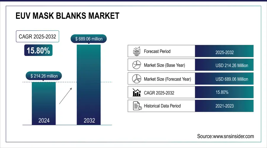
The EUV Mask Blanks Market Size was valued at USD 214.26 million in 2024 and is expected to reach USD 689.06 million by 2032 and grow at a CAGR of 15.80 % over the forecast period 2025-2032.
The EUV mask blanks market growth is driven primarily due to the strong emphasis by the semiconductor industry on innovation and investment in next-generation EUV lithography for the manufacturing of chips. Rising demand for smaller and more powerful chips in consumer electronics, automotive and data centers is also driving growth, with a push by the government to ramp up domestic semiconductor production.
Market Size and Forecast:
-
EUV Mask Blanks Market Size in 2024: USD 214.26 Million
-
EUV Mask Blanks Market Size by 2032: USD 689.06 Million
-
CAGR: 15.80% from 2025 to 2032
-
Base Year: 2024
-
Forecast Period: 2025–2032
-
Historical Data: 2021–2023
To Get more information on EUV-Mask-Blanks-Market - Request Free Sample Report
Key EUV Mask Blanks Market Trends
-
Growing adoption of EUV lithography in advanced semiconductor manufacturing is driving demand for high-quality EUV mask blanks with superior defect control and optical properties.
-
Rising demand for 3nm and sub-3nm process nodes is pushing manufacturers to invest in defect-free mask blanks that support extreme precision and high reflectivity.
-
Integration of multilayer coatings and advanced absorber materials is improving pattern fidelity, critical dimension control, and overall imaging performance.
-
Increasing collaboration between mask blank producers and semiconductor foundries is accelerating innovation in defect inspection and metrology solutions.
-
Development of pellicle-protected EUV mask blanks is gaining momentum to enhance mask durability and extend operational lifespans in high-volume manufacturing.
-
Advancements in High-NA EUV lithography are creating new opportunities for specialized mask blank materials that enable improved throughput and reduced line-edge roughness.
-
Government and industry investments in chip manufacturing infrastructure are fostering regional production capabilities and strengthening supply chain resilience for EUV mask blanks.
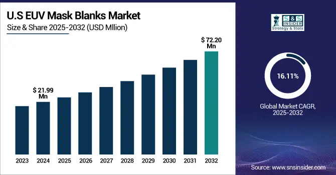
U.S. EUV Mask Blanks Market
The U.S. EUV Mask Blanks Market size was USD 21.99 million in 2024 and is expected to reach USD 72.20 million by 2032, growing at a CAGR of 16.11 % over the forecast period of 2025–2032.The growth is driven by the rising adoption of EUV lithography in next-generation semiconductor manufacturing, especially for 3nm and smaller nodes. Increasing investments by chipmakers in advanced materials, defect-free mask technologies, and multilayer coating innovations are enhancing yield performance and production efficiency in U.S. fabs.
EUV Mask Blanks Market Growth Drivers
-
Increasing adoption of EUV lithography for advanced semiconductor manufacturing boosts market demand significantly
Increasing penetration of EUV lithography in the semiconductor production process is boosting the EUV mask blanks market. EUV technology makes faster and denser bigger semiconductor nodes possible with higher precision, which is essential for next-generation chips. This adoption means fewer defects and higher wafer yields, luring chip manufacturers to pour money into EUV mask blanks. Moreover, rising adoption in high performance computing, AI, and 5G technologies drive the demand of advanced mask blanks, leading the market to grow during the forecast period.
According to research, More than 70% of advanced logic chips for AI accelerators and 5G base stations utilize EUV lithography in their fabrication.
EUV Mask Blanks Market Restraints
-
High manufacturing costs and complex fabrication processes limit EUV mask blanks market growth
EUV mask blanks are expensive to manufacture, due to the high cost of materials, the need for sophisticated and complicated processing equipment and processes. These costs can be a significant factor preventing EUV from being widely adopted at smaller- and mid-size chip manufacturers. Moreover, because of the complicated mask blank fabricating procedures, the quality control and defect management should be strictly taken to make the operation more difficult. These cost and process barriers limit wider uptake and decelerate growth despite new technological developments.
EUV Mask Blanks Market Opportunities
-
Technological advancements in mask blank materials and coating processes enable market innovation
Continuous R&D activities in the improvement of mask blank materials and advanced coating technologies is lucrative. Better mask durability, less defect, improved reflectivity can all assist lithography performance and wafer yield. Mask blanks are even using more and more novel materials and nanotechnology which can provide new application fields and enhance the market competition. Firms that are adopting innovative solutions can leverage the growing needs for advanced semiconductor manufacturing. Furthermore, partnerships between private companies and research institutions are anticipated to hasten the commercialization of innovative solutions and reinforce long-term growth prospects in worldwide markets.
According to research, Advanced coatings have improved mask durability by up to 30% and reduced defect rates by 25%, resulting in wafer yield increases of 15%.
EUV Mask Blanks Market Challenges:
-
Maintaining ultra-low defect rates in EUV mask blanks manufacturing remains a persistent challenge
The ultra-low defect density needed for EUV mask blanks is very difficult to achieve because EUV lithography is highly sensitive to the tiniest defects. Even small flaws can cause wafers to fail and yield to drop. Factory owners must spend billions on advanced inspection, cleaning and repair tools, adding expense and complexity. Maintaining high quality even during production scaleup is a continuous challenge that may affect market growth. Additionally, the scarcity of faultless raw materials adds another layer of complexity to production, requiring more precision and stricter process control throughout production.
EUV Mask Blanks Market Segment Analysis:
By Type
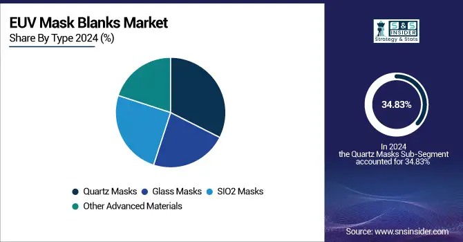
Quartz Masks segment dominated the EUV Mask Blanks Market share of about 34.83% in 2024. This is primarily because of the very good thermal and optical properties of quartz which guarantee negligible distortion upon high energetic EUV exposure. A quartz mask is strong and stable enough to withstand harsh conditions in semiconductor manufacturing with EUV lithography. Key players such as AGC Inc. have established a firm position in this market by supplying high-purity quartz products for critical mask applications.
Glass Masks segment is expected to grow at the fastest CAGR of about 16.96% from 2025-2032. This development is driven by continued advancement in the glass substrate material, which increases light transmittance, while at the same time it lowers production cost. Firms such as Shenzhen Newway Photomask are developing higher level of glass mask technologies as cost-effective substitutes for quartz, especially in less traditional markets and applications. The use of glass masks is ramping in a variety of fabs, as chipmakers continue to search for more scalable lithography options.
By Application
Semiconductor Manufacturing segment dominated the EUV Mask Blanks Market with the highest revenue share of about 41.38% in 2024. This dominance is due to the extensive implementation of the EUV lithography in advanced chip making, which is fueled by the ever-growing need for smaller nodes and the higher transistor density. Continued chip design innovation, performance and low energy requirements are further driving the semiconductor market’s demand for EUV mask blanks.
MEMS segment is expected to grow at the fastest CAGR of about 17.19% from 2025-2032. This rapid growth is driven by the increasing use of MEMS technology for IoT, wearable devices, medical devices, and automotive sensors. The euv mask blanks companies, such as SUSS MicroTec, have invested considerably in sophisticated lithography systems which have been specifically optimized for MEMS fabrication. With the requirement of device miniaturization and more and more emphasis on precision, the MEMS manufacturing highlights EUV mask blank to provide high resolution and accuracy, further promoting the application of EUV in this field.
By Production
The EUV-Specific Production Techniques segment dominated the EUV Mask Blanks Market with the highest revenue share of about 37.29% in 2024. This dominance is because of the increasing demand for high precision defect-free mask blanks for EUV lithography. These technologies provide the best light transmission and pattern integrity that are vital to serve modern semiconductor designs. Hoya Corporation and others have pounced on this opportunity, offering EUV mask blanks optimized for the strict requirements imposed by next-generation chip manufacturing.
Hybrid Production Techniques segment is expected to grow at the fastest CAGR of about 17.05% from 2025-2032. The growth is attributed to the growing demand for cost-effective, high-production processes which include conventional and advanced production scenes. Photronics, Inc., for instance, is working on hybrid techniques and approaches that provide manufacturing agility and enhanced yield, all while maintaining high quality. Hybrid production approach becomes more attractive as performance and cost requirements are balanced by mid-tier semiconductor fabs driving its market expansion.
By End-User Industry
Consumer Electronics segment dominated the EUV Mask Blanks Market with the highest revenue share of about 41.90% in 2024. The main reason is the strong demand for smartphones, tablets, wearables, and other small and light high performance devices that use highly developed semiconductor components. We will continue to see tech giants, such as Samsung Electronics, push the limits of EUV lithography to provide the latest and greatest consumer products, thus providing a major source of demand for stable, high-quality EUV mask blanks in this field.
The Automotive Electronics segment is expected to grow at the fastest CAGR of about 17.39% from 2025-2032. The growing proportion of semiconductors in cars, particularly for autonomous driving, ADAS, EV power systems has also driven demand for advanced chips. Players such as Infineon Technologies are increasingly adopting the advanced lithography to address the demanding automotive-grade electronics quality and reliability requirements. This escalation is quickly driving the need of EUV mask blanks for high-performance automotive applications.
EUV Mask Blanks Market Regional Analysis
Asia Pacific EUV Mask Blanks Market Insights
Asia Pacific region dominated the market share of approximately 40.83% in the EUV Mask Blanks Market in 2024, mainly driven by the companys robust semiconductor manufacturing industry and large investments into EUV lithography infrastructure in the region. Nations including Taiwan, South Korea and Japan are home to leading chip manufacturers like TSMC and Samsung, which leads the race to develop advanced nodes. The geographical proximity of these manufacturing plants also ensures the abundance of qualified labor force and technological know-how and cements Asia Pacific as the frontrunner.

Get Customized Report as per Your Business Requirement - Enquiry Now
-
China leads the Asia Pacific EUV mask blanks market on account of well-established government policies, significant investments in semiconductor infrastructure, and increasing requirement for chip manufacturing. And its emphasis on technological autonomy enhances its influence in the region.
North America EUV Mask Blanks Market Insights
North America is projected to grow at the fastest CAGR of about 17.24% from 2025 to 2032, fueled by rising domestic chip production and government-led efforts to boost semiconductor self-reliance. With the presence of tech giants such as the Intel Corporation and increasing investment in EUV mask blank fabs, demand for advanced mask blanks is on the rise. Besides, initiatives implemented for diminishing reliance on foreign sources and fostering innovation in AI and high-performance computing domains are also promoting the EUV mask blank sales in the region.
-
The U.S. dominates the North America EVS Blank Market owing to its developed semiconductor R&D infrastructure, heavy investment in EVS technology, and supportive government policies for increasing domestic chip production to minimize dependence on overseas semiconductor supply chains.
Europe EUV Mask Blanks Market Insights
Europe contributes significantly to the EUV Mask Blanks Market, as a result of the region’s concentration on high-precision manufacturing and advanced materials. Innovation: The region’s mature semiconductor equipment industry, coupled with substantial government funding and collaboration in research activities. This stable growth in the EUV mask blanks business is being driven by Europe’s focus on the reinforcement of its semiconductor supply chain and technological autonomy.
-
Germany Leading in Europe because of the strong industrial base, excellent semiconductor research and strategic investments. Stressing on its technological innovation and working closely with key industry players give it the edge over the other European nations.
Middle East & Africa & Latin America (LATAM) EUV Mask Blanks Market Insights
The Middle East & Africa Market has been dominated by UAE owing to the strong government support and funding for the research & development of advanced manufacturing technologies. Brazil is leading the way in Latin America with a larger industrial base and an increasing attention on semiconductor development, followed by other countries slowly getting into the sector.
Competitive Landscape for EUV Mask Blanks Market
Applied Materials, Inc.
Applied Materials, Inc. is a global leader in materials engineering solutions used to produce virtually every new chip and advanced display in the world. The company focuses on enabling the semiconductor industry’s transition to advanced nodes through innovative patterning, deposition, and metrology technologies that support EUV and High-NA EUV lithography.
-
-
In February 2024, Applied Materials introduced a portfolio of products and solutions specifically designed to address the patterning requirements of chips in the “angstrom era.” These innovations aim to overcome critical EUV and High-NA EUV challenges such as line edge roughness and edge placement errors, thereby enhancing precision and yield in next-generation semiconductor manufacturing.
-
Dai Nippon Printing Co., Ltd. (DNP)
Dai Nippon Printing Co., Ltd. (DNP) is a leading manufacturer of high-performance photomasks and mask blanks used in advanced semiconductor production. The company is actively investing in EUV technology to meet the growing demand for miniaturized, high-performance devices in the 3-nanometer and below process nodes.
-
-
In December 2023, DNP developed a new photomask manufacturing process for 3-nanometer EUV lithography, enabling the production of highly precise and smaller node semiconductors. This development supports the semiconductor industry’s push toward higher performance, lower power consumption, and continued device miniaturization.
-
EUV Mask Blanks Market Key Players
Some of the EUV Mask Blanks Market Companies
- AGC Inc.
- Hoya Corporation
- S&S Tech Co., Ltd.
- Applied Materials, Inc.
- Photronics Inc.,
- Toppan Photomasks Inc.
- Shin-Etsu Chemical Co., Ltd.
- Dai Nippon Printing Co., Ltd.
- Nippon Filcon Co., Ltd.
- Compugraphics International Ltd.
- SUMCO Corporation
- GlobalWafers Co., Ltd.
- Wafer World, Inc.
- Daxin Materials, Inc.
- Siltronic AG
- ATMI, Inc. (part of Entegris)
- MEMS Optical, Inc.
- SKC Co., Ltd.
- Lasertec Corporation
- Carl Zeiss SMT GmbH
| Report Attributes | Details |
|---|---|
| Market Size in 2024 | USD 214.26 Million |
| Market Size by 2032 | USD 689.06 Million |
| CAGR | CAGR of 15.80% From 2025 to 2032 |
| Base Year | 2024 |
| Forecast Period | 2025-2032 |
| Historical Data | 2021-2023 |
| Report Scope & Coverage | Market Size, Segments Analysis, Competitive Landscape, Regional Analysis, DROC & SWOT Analysis, Forecast Outlook |
| Key Segments | • By Type (Quartz Masks, Glass Masks, SIO2 Masks, Other Advanced Materials) • By Application (Semiconductor Manufacturing, MEMS (Micro-Electro-Mechanical Systems), Nanotechnology Applications, Optical Components) • By End-User Industry (Consumer Electronics, Automotive Electronics, Telecommunications, Healthcare & Medical Devices) • By Production (Conventional Production Techniques, EUV-Specific Production Techniques, Hybrid Production Techniques, Automated Production Systems) |
| Regional Analysis/Coverage | North America (US, Canada), Europe (Germany, France, UK, Italy, Spain, Poland, Russsia, Rest of Europe), Asia Pacific (China, India, Japan, South Korea, Australia,ASEAN Countries, Rest of Asia Pacific), Middle East & Africa (UAE, Saudi Arabia, Qatar, South Africa, Rest of Middle East & Africa), Latin America (Brazil, Argentina, Mexico, Colombia Rest of Latin America) |
| Company Profiles | AGC Inc., Hoya Corporation, S&S Tech Co., Ltd., Applied Materials, Inc., Photronics Inc., Toppan Photomasks Inc., Shin-Etsu Chemical Co., Ltd., Dai Nippon Printing Co., Ltd., Nippon Filcon Co., Ltd., Compugraphics International Ltd. |
Frequently Asked Questions
Asia Pacific dominated the EUV Mask Blanks Market in 2024.
Semiconductor Manufacturing segment dominated the EUV Mask Blanks Market.
The major growth factor of the EUV Mask Blanks Market is the increasing demand for advanced semiconductor chips requiring precise EUV lithography for smaller, efficient devices.
The EUV Mask Blanks Market size was USD 214.26 billion in 2024 and is expected to reach USD 689.06 billion by 2032.
The EUV Mask Blanks Market is expected to grow at a CAGR of 15.80 % from 2025-2032.
Get in Touch
