PPLN Chip Market Report Scope and Overview:
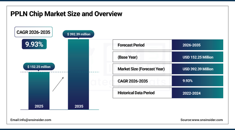
The PPLN Chip Market size was valued at USD 152.25 Million in 2025 and is expected to reach USD 392.39 Million by 2035, growing at a CAGR of 9.93% over the forecast period of 2026-2035.
The PPLN (Periodically Poled Lithium Niobate) Chip Market is witnessing important growth since demand is rising for high-performance photonic components within AI, quantum computing, and telecommunications. Efficient frequency conversion, quantum signal processing, and nonlinear optics depend on PPLN chips. These technologies are important for next-generation chip architectures. PPLN adoption is being pushed onward by the need for scalable, low-loss, compact optical solutions as AI infrastructure and semiconductor manufacturing global investments accelerate. Advanced computing systems are critically enabled through their integration into AI accelerators, optical links, and telecom networks. Consistent market expansion is expected to occur because of technological advancements in thin-film PPLN and waveguide integration.
TSMC’s USD 100 Billion U.S. investment in advanced AI chip manufacturing is expected to significantly boost demand for PPLN chips used in quantum optics and photonic integration. As next-gen AI systems require high-efficiency frequency conversion, PPLN technologies will play a vital role in meeting performance and scalability needs.
PPLN Chip Market Size and Forecast:
-
Market Size in 2025: USD 152.25 Million
-
Market Size by 2035: USD 392.39 Million
-
CAGR: 9.93% from 2026 to 2035
-
Base Year: 2025
-
Forecast Period: 2026–2035
-
Historical Data: 2022–2024
To Get More Information On PPLN Chip Market - Request Free Sample Report
PPLN Chip Market Highlights:
-
Commercial traction with Quantum Computing Inc receiving multiple purchase orders for thin-film lithium niobate (TFLN) photonic chips from European and Canadian clients, showing real-world market demand
-
QCi shipped its first commercial entangled photon source, marking progress from research prototypes to real-world deployment
-
PPLN/TFLN chip demand spans North America, Europe, and Asia, with QCi’s U.S. foundry in Arizona set for full-scale production in 2025 to accelerate commercialization
-
Growth is fueled by quantum frequency conversion needs, scalable photonic integration, and rising adoption of PPLN chips for secure communications, AI photonics, and telecom wavelength conversion
-
Increasing demand for thin-film lithium niobate photonic chips is opening new avenues for commercial adoption beyond research labs in telecom, AI, and cybersecurity applications
-
PPLN/TFLN chips offer high optical nonlinearity, low power consumption, and compact integration, making them ideal for next-generation photonic integrated systems
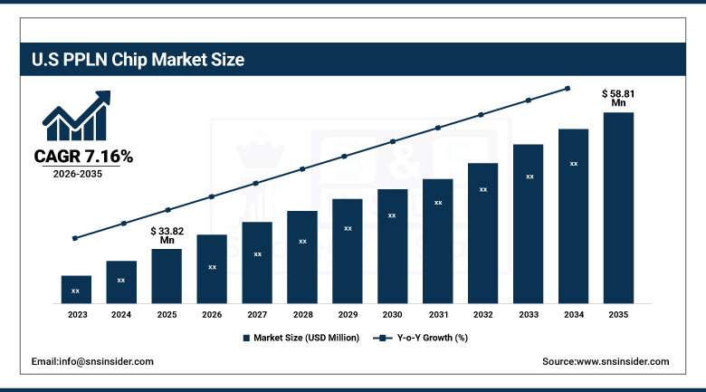
The U.S PPLN Chip Market Size was valued at USD 33.82 Million in 2025 and is expected to reach USD 58.81 Million by 2035 and grow at a CAGR of 7.16% over the forecast period 2026-2035. The PPLN chip market growth is driven by rising demand for frequency conversion in quantum computing, AI, and telecom. The PPLN chip market trends include integration of thin-film lithium niobate, photonic chips, and government-backed semiconductor manufacturing initiatives.
PPLN Chip Market Drivers:
-
Increasing Demand for Efficient Frequency Conversion Pushes PPLN Chip Growth
The demand for ultra-efficient quantum frequency conversion is one of the many catalysts driving the PPLN chip market today. Periodically poled thin-film lithium niobate (PPLN) waveguides allow for nearly seamless wavelength conversion of single photons in the system, which is key to linking quantum memories with telecom infrastructure. PPLN solutions boast bidirectional conversion efficiencies of up to 90% and minimal noise interrupting the transfer, and PPLN technology is essential to the future development of scalable quantum communication systems. The attributes of compact integration, low power consumption, and high optical nonlinearity of PPLN chips open opportunities for use in quantum networks, AI photonics, and secure data release. With the evolving demand for reliable frequency translation in high-speed optical systems, the rate of adoption of PPLN technology is expected to accelerate in the telecom and quantum memory industries.
Researchers produced a quantum frequency converter using a ring–Mach Zehnder interferometer employing thin-film PPLN and achieved 90% bidirectional conversion of photons. The apparatus facilitates ultra-low-noise signal transfer from visible-spectrum quantum memories to telecom networks.
PPLN Chip Market Restraints:
-
Complex Fabrication and High Costs Slow Down Growth of the PPLN Chips Market
The PPLN chip market is experiencing escalating demand, but there are multiple key inhibitors that impede the broad adoption of this technology. Primarily, the fabrication obstacles are a challenge; in particular, ensuring a uniform periodic poling at the nanoscale for thin-film lithium niobate structures is particularly difficult. The challenge becomes more difficult when acknowledging manufacturing irregularities in PPLN chips. Manufacturing inconsistencies lead to lower conversion efficiency, increased optical loss, and deterioration over the scale of the thickness of the device. Additional limitations are the high price of raw materials and sophisticated fabrication equipment made for a high cost of production, price points tying these projects out of reach for smaller photonics start-ups and research labs.
Other limitations related to the technical challenges of integrating PPLN chips into existing semiconductor platforms. Hybrid systems require careful thermal and optical management. Supply of foundries producing thin-film lithium niobate devices is limited, and therefore, prototyping is hindered and commercialization timelines slow. Another key restraint is the relatively 'niche' nature of end-use applications, and aspects of quantum communication, advanced telecom and AI photonics remain in development and segments are not expected to commercialize. Additionally, large-scale deployment of this technology is also restricted by asymmetries in packaging and testing standardized methods. In summary, three approaches are needed to move the PPLN chip technology into more utility amenable for photonic applications.
PPLN Chip Market Opportunities:
-
Growing Demand for Photonic Integration Creates Opportunities in the PPLN Chip Market
The increasing demand for thin-film lithium niobate (TFLN) photonic chips is opening new growth avenues for the PPLN chip market. As many industries continue to adopt integrated photonic capabilities in applications including telecom, AI, and cybersecurity, PPLN structures are gaining traction as they are efficient for optical frequency conversion and the creation of entangled photons. Clients who were formally using PPLN chips in the lab or for research are starting to ramp up into commercial orders as seen with recent orders. This indicates that more and more projects are transitioning from research into real-world, commercial deployment. The unique ability for PPLN chips to provide scalable functionality, low power consumption, and high-speed processing makes them a good candidate for moving into the next generation of photonic integrated systems, which is why they present great opportunities for manufacturers and developers to increase their presence in higher end, application-specific photonic chip solutions.
On January 8, 2025 - Quantum Computing Inc. announced additional new orders for its thin-film lithium niobate (TFLN) photonic chips from European and Canadian clients, which again demonstrates continuing interest in the commercial space. Our recent orders are fulfilling a rising demand for PPLN-based solutions for frequency conversion and entangled photon generation for a range of telecom, AI, and other application spaces.
PPLN Chip Market Segment Analysis:
By Type
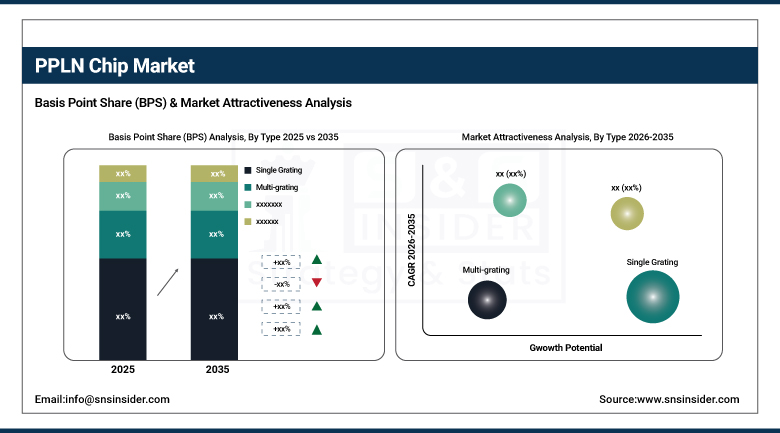
In 2025, the Single Grating segment holds the largest PPLN chip market at approximately 47%, fueled by growing demand for precise optical control. The use of PPLN waveguide chips significantly improves efficiency through advanced frequency conversion and nonlinear optics, driving adoption in industrial sensing, laser applications, and high-speed photonic systems.
The Multi-Grating segment is projected to witness the fastest growth in the PPLN chip market over 2026-2035, registering a CAGR of 12.23%. This surge is propelled by the rising need for high-resolution beam control and the expanding use of PPLN waveguide chips in precision optics and next-generation photonic technologies.
By Application
In 2025, the Telecommunications segment commands the largest PPLN chip market share of around 42%, driven by the rising need for high-speed data transmission and wavelength conversion. The integration of PPLN waveguide chips enables efficient signal modulation and frequency control, making them essential for advanced fiber-optic networks and next-generation telecom infrastructure.
The Quantum Optics segment is projected to witness the fastest growth in the PPLN chip market over 2026-2035, with a CAGR of 15.41%. This surge is fueled by increasing adoption of PPLN waveguide chips for entangled photon generation, quantum frequency conversion, and ultra-low-noise operations in emerging quantum computing and communication technologies.
By End-Use Industry
In 2025, the Telecommunications segment commands the PPLN chip market share at around 44%, driven by rising demand for high-speed data transmission and wavelength conversion. PPLN waveguide chips play a crucial role in enabling efficient optical signal processing, supporting advanced telecom infrastructure, including 5G and fiber-optic networks.
The Defense & Aerospace segment is projected to witness the fastest growth in the PPLN chip market over 2026-2035, with a CAGR of 12.51%. This surge is fueled by rising deployment of PPLN waveguide chips in secure quantum communication, precision LIDAR, and next-gen sensing systems vital for mission-critical defense, aerospace navigation, and surveillance technologies.
PPLN Chip Market Regional Analysis:
North America PPLN Chip Market Trends:
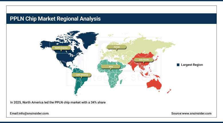
In 2025, North America led the PPLN chip market with a 34% share, driven by strong investments in quantum research, advanced telecommunications infrastructure, and defense modernization. The region’s dominance is supported by the presence of key players, robust photonic R&D ecosystems, and early adoption of PPLN waveguide chips in high-performance optical applications.
Researchers at University of Twente and City University of New York demonstrated integrated Brillouin photonics on thin-film lithium niobate, achieving a 20 nm tuning range, 9 Hz laser linewidth, and over 3 dB net SBS gain in a 10 cm waveguide, highlighting North America’s innovation in scalable, ultra‑low noise photonic chip platforms.
The PPLN chip market in the U.S. is expanding rapidly, driven by breakthroughs in thin-film lithium niobate technologies, strong research infrastructure, and growing demand across telecom, defense, and quantum applications.
Get Customized Report as Per Your Business Requirement - Enquiry Now
Asia-Pacific PPLN Chip Market Trends:
Asia Pacific is expected to witness the fastest growth in the PPLN chip market over 2026-2035, with a projected CAGR of 12.36%. This surge is driven by rapid advancements in photonics research, increased investments in optical communication infrastructure, and rising demand for PPLN waveguide chips across telecom, quantum computing, and industrial sensing applications.
Europe PPLN Chip Market Trends:
In 2025, Europe emerged as a promising region in the PPLN chip market, driven by growing investments in photonic research, rising demand for quantum communication technologies, and expanding industrial automation. Supportive EU initiatives and collaborations between research institutions and photonics startups are accelerating innovation, positioning Europe as a key player in the global market.
Wolfspeed has officially shelved its USD 3 billion chip factory project in Ensdorf, Germany, citing slower EV adoption. The move marks a setback for Europe’s semiconductor independence efforts.
Latin America andMiddle East & Africa PPLN Chip Market Trends:
Latin America and the Middle East & Africa (MEA) are experiencing steady growth in the PPLN chip market, supported by emerging telecom infrastructure, growing interest in quantum optics, and government-led digitization efforts. Rising investments in photonics research and industrial automation are gradually enhancing regional adoption of PPLN waveguide chips across key sectors.
PPLN Chip Market Competitive Landscape:
Quantum Computing Inc., established in 2018, is a leading developer of thin-film lithium niobate (TFLN) photonic chips and quantum photonic solutions. The company focuses on high-efficiency frequency conversion, entangled photon sources, and scalable photonic integrated circuits, serving research, telecom, AI, and secure communication markets worldwide with innovative quantum-enabled technologies.
-
In January 2025: Quantum Computing Inc. (QCi) secured its third and fourth purchase orders for its TFLN photonic chip foundry, concluding its 2024 Pilot Launch Program. Full-scale production at the Tempe, Arizona facility is set to begin in Q1 2025.
PPLN Chip Market Key Players:
-
Quantum Computing Inc.
-
Optilab
-
HC Photonics
-
Covesion
-
Gooch & Housego PLC
-
Coherent, Inc.
-
Thorlabs, Inc.
-
Newport Corporation
-
IPG Photonics Corporation
-
Cristal Laser S.A.
-
NTT Electronics
-
AdvR
-
TOPTICA Photonics AG
-
Lightwave Logic
-
Alps Electric Co., Ltd.
-
Lumibird Group
-
Altechna
-
Jenoptik AG
-
Oxford Instruments
-
Photonics Industries International
| Report Attributes | Details |
|---|---|
| Market Size in 2025 | USD 152.25 Million |
| Market Size by 2035 | USD 392.39 Million |
| CAGR | CAGR of 9.93% From 2026 to 2035 |
| Base Year | 2025 |
| Forecast Period | 2026-2035 |
| Historical Data | 2022-2024 |
| Report Scope & Coverage | Market Size, Segments Analysis, Competitive Landscape, Regional Analysis, DROC & SWOT Analysis, Forecast Outlook |
| Key Segments | • By Type (Single Grating, Multi-grating, Fanout Grating) • By Application (Telecommunications, Photonics, Quantum Optics, Biomedical & Healthcare, Others) • By End Use Industry (Telecommunication Service Providers, Research Institutes & Laboratories, Defense & Aerospace, Healthcare & Biomedical Institutions, Others) |
| Regional Analysis/Coverage | North America (US, Canada), Europe (Germany, UK, France, Italy, Spain, Russia, Poland, Rest of Europe), Asia Pacific (China, India, Japan, South Korea, Australia, ASEAN Countries, Rest of Asia Pacific), Middle East & Africa (UAE, Saudi Arabia, Qatar, South Africa, Rest of Middle East & Africa), Latin America (Brazil, Argentina, Mexico, Colombia, Rest of Latin America). |
| Company Profiles | Quantum Computing Inc., Optilab, HC Photonics, Covesion, Gooch & Housego PLC, Coherent, Inc., Thorlabs, Inc., Newport Corporation, IPG Photonics Corporation, Cristal Laser S.A., NTT Electronics, AdvR, TOPTICA Photonics AG, Lightwave Logic, Alps Electric Co., Ltd., Lumibird Group, Altechna, Jenoptik AG, Oxford Instruments, Photonics Industries International. |
Frequently Asked Questions
North America dominated the PPLN Chip Market in 2025.
The “Single Grating” segment dominated the PPLN Chip Market.
Rising demand for efficient frequency conversion in quantum computing and telecom drives the PPLN chip market.
The PPLN Chip Market size was valued at USD 152.25 Million in 2025 and is expected to reach USD 392.39 Million by 2035
The PPLN Chip Market is expected to grow at a CAGR of 9.93%during 2026-2035.
Get in Touch
