Probe Cards Market Report Scope & Overview:
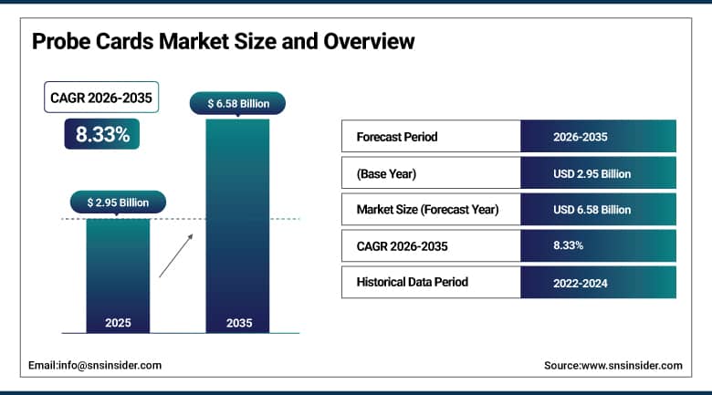
The Probe Cards Market was valued at USD 2.95 billion in 2025 and is expected to reach USD 6.58 billion by 2035, growing at a CAGR of 8.33% from 2026–2035.
Probe cards form the physical bridge between wafer test equipment and semiconductor dies, enabling engineers to verify electrical functionality before costly packaging steps. As chip architectures shrink below three nanometres and chiplet-based designs proliferate, the mechanical and electrical demands on probe cards escalate sharply. Higher pin counts, sub-60-micrometre pitches, multi-site simultaneous contact, and signal integrity at frequencies beyond 56 gigahertz are becoming standard requirements. Government semiconductor incentive packages, including the U.S. CHIPS Act and Europe's Chips Act, are accelerating fab construction timelines and front-loading test equipment orders, providing a direct near-term revenue catalyst for the probe card sector.
Probe Cards Market Size and Forecast
-
Market Size in 2025: USD 2.957 Billion
-
Market Size by 2035: USD 6.583 Billion
-
CAGR: 8.33% from 2026 to 2035
-
Base Year: 2025
-
Forecast Period: 2026–2035
-
Historical Data: 2022–2024
To Get More Information On Probe Cards Market - Request Free Sample Report
Probe Cards Market Trends
-
Transition from cantilever to MEMS architectures accelerating as sub-three-nanometre nodes require contact uniformity that conventional spring-tip probes cannot reliably maintain.
-
Advanced packaging and chiplet integration shifting more test activity to wafer level, raising per-device probe card content and frequency of card replacement.
-
AI accelerator demand creating need for cards capable of testing high-bandwidth memory and logic at frequencies and pin densities previously reserved for specialty applications.
-
Double-sided wafer probing solutions emerging for silicon photonics and backside power delivery architectures that single-sided cards cannot address.
-
Modular, field-replaceable probe card designs gaining traction as fabs seek to reduce downtime and spread replacement costs over longer service intervals.
-
AI-assisted alignment systems shortening setup cycles by approximately 30% and achieving near-perfect first-touchdown contact rates on advanced cards.
-
Japanese suppliers expanding capacity significantly to serve domestic fab ramp-ups and export demand for ultra-fine-pitch probe solutions.
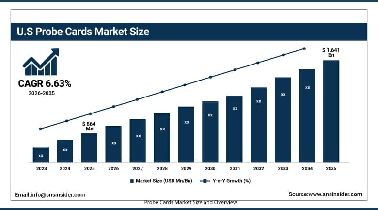
U.S. Probe Cards Market Size Outlook:
The U.S. Probe Cards Market was valued at USD 864 million in 2025 and is expected to reach USD 1.641 billion by 2035 at a CAGR of 6.63%, driven by AI chip development, 5G silicon programmes, and silicon photonics test requirements at leading U.S. semiconductor design and foundry operations.
Probe Cards Market Segment Insights
-
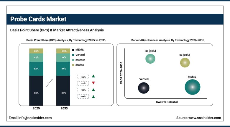
By Technology, MEMS probe cards accounted for approximately 36% of revenue in 2025 and dominate through signal integrity and precision advantages; MEMS-Vertical variants are the fastest-growing technology at approximately 9.17% CAGR, driven by sub-60-micrometre pitch requirements at advanced nodes.
-
By Application, Foundry and Logic held approximately 35% share in 2025 as the dominant application owing to AI, 5G, and HPC chip demand; DRAM is the fastest-growing application as high-bandwidth memory requirements for AI accelerators drive testing intensity.
-
By Type, Advanced Probe Cards dominate as semiconductor complexity pushes standard cards out of leading-edge production; Standard Probe Cards retain relevance in mature node, parametric, and cost-sensitive test environments.
-
By End-User, Foundries held the largest share owing to high wafer volumes and multi-customer device diversity; OSATs are the fastest-growing end-user as chiplet assembly migrates outside captive fabs.
-
By Wafer Size, 300mm wafer probing dominates reflecting mainstream production volumes; 450mm is a future-oriented segment currently in early development alongside the next industry node transition.
By Technology: MEMS dominates, Vertical MEMS grows fastest
MEMS probe cards hold the largest technology share because microfabrication techniques produce tip arrays with consistent contact force, fine pitch capability, and long service life that conventional wire-formed cantilever probes struggle to match at advanced nodes. Vertical MEMS is the segment accelerating most rapidly. TSMC's volume production of the two-nanometre gate-all-around process, Intel's 18A backside power delivery, and the growth of chiplet interconnects exceeding 100 pads per square millimetre all demand pitch tolerances and contact repeatability that only vertical MEMS architecture reliably delivers. FormFactor's sub-60-micrometre pitch platform launched in 2025 illustrates where the technology frontier currently sits.
By Application: Foundry and Logic dominates, DRAM grows fastest
Foundry and logic test remains the single largest revenue pool because every high-performance computing, AI training, and 5G chip produced at leading foundries needs thorough wafer-level electrical verification before packaging. DRAM is growing fastest because the AI infrastructure boom is driving extraordinary demand for high-bandwidth memory, which in turn requires intensive probe-based testing at increasingly fine geometries and higher parallelism. Each generation of DRAM pushes density and access speed higher, translating directly into probe card specification upgrades and more frequent card replacement cycles.
By End-User: Foundries dominate, OSATs grow fastest
Foundries are the primary buyers because they operate the largest volume of active probe stations and serve the broadest range of device types from a single test floor. Outsourced semiconductor assembly and test providers are growing fastest as the chiplet ecosystem matures. When chip companies disaggregate compute and memory dies and assemble them through advanced packaging contractors, OSAT facilities must test individual chiplets at wafer level before they become components in larger stacks. This structural shift in the semiconductor supply chain is pulling a growing share of wafer-level test work into OSAT operations that were previously focused on final test only.
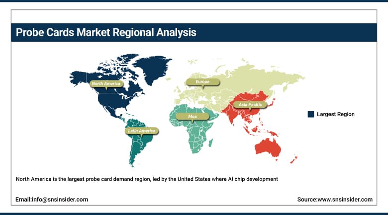
Probe Cards Market Regional Analysis:
|
Region |
Major Country |
Share within Region (%) |
|---|---|---|
|
North America |
United States |
~80% |
|
Europe |
Germany |
~30% |
|
Asia Pacific |
Taiwan |
~45% |
|
Middle East & Africa |
Israel |
~28% |
|
Latin America |
Brazil |
~42% |
North America Probe Cards Market Insights
North America is the largest probe card demand region, led by the United States where AI chip development, 5G silicon programmes, silicon photonics, and CHIPS Act-funded fab capacity additions are sustaining robust test equipment investment across design companies, foundries, and test subcontractors.
Get Customized Report as Per Your Business Requirement - Enquiry Now
Asia Pacific Probe Cards Market Insights
Asia Pacific is the fastest-growing region, anchored by Taiwan's foundry ecosystem, South Korea's memory industry, and Japan's expanding domestic fab base. Governments across the region are incentivising semiconductor manufacturing capacity, pulling forward demand for probe card procurement across multiple national programmes.
Europe Probe Cards Market Insights
Europe's EUR 43 billion Chips Act is funding new semiconductor manufacturing facilities that will progressively build European probe card demand. Specialty probe applications in automotive silicon, industrial sensors, and European space programmes provide a differentiated demand base distinct from the high-volume logic and memory markets of Asia.
Probe Cards Market Growth Drivers:
-
Semiconductor complexity and miniaturisation demanding progressively higher probe card precision, pin density, and signal integrity at every new technology node.
With each process generation, die dimensions shrink, pad pitches tighten, and electrical test frequencies rise. Probe cards must keep pace or yield losses escalate. This technology-driven replacement cycle is structural and largely immune to demand volatility in end markets, because chipmakers cannot afford to ship unverified wafers regardless of macroeconomic conditions.
FormFactor's SmartMatrix 100 platform and the Teradyne-ficonTEC dual-sided silicon photonics probe test cell announced in April 2025 represent two inflection points that expand addressable probe card revenue well beyond traditional silicon testing into photonic integrated circuit qualification, directly addressing the growing overlap between semiconductor and communications hardware industries.
Probe Cards Market Restraints
-
High unit cost and limited useful life at advanced nodes increasing per-wafer test cost and creating budget pressure for foundries managing tight capital allocation.
Advanced MEMS probe cards cost considerably more than cantilever alternatives and wear out faster when contact densities are high. For foundries operating on thin process margins, frequent card replacement represents a meaningful operating cost that drives engineering investment in card longevity improvements and alternative test strategies.
Probe Cards Market Opportunities
-
Silicon photonics, automotive power semiconductors, and wafer-level burn-in creating three distinct high-growth application frontiers beyond the traditional logic and memory markets.
Silicon photonics probe testing requires simultaneous optical alignment and electrical probing, a capability gap that Teradyne and ficonTEC have begun addressing commercially. Automotive power semiconductors demand testing across wide temperature and voltage ranges that standard probe infrastructure handles poorly. Wafer-level burn-in, where stress testing occurs before packaging to screen infant mortality failures, represents a third frontier where probe cards enable significant quality improvement at a cost that scales well with volume production.
Recent Developments:
-
April 2025: Teradyne and ficonTEC unveiled the first high-volume double-sided wafer probe test cell for silicon photonics, integrating UltraFLEXplus ATE with optical alignment for scalable electro-optical testing in AI and data center applications.
-
February 2025: Nidec Advance Technology participated in SEMICON Korea 2025, showcasing advanced probe cards and power semiconductor inspection systems targeting EV and HEV applications.
-
2025: FormFactor launched its sub-60-micrometre pitch SmartMatrix platform for chiplet interconnect probing, enabling fabs to test advanced packaging architectures exceeding 100 pads per square millimetre.
-
2024: FormFactor acquired TESTiN Technologies to deepen its logic and memory probe card portfolio for next-generation semiconductor architectures.
-
2025: Japanese probe card suppliers expanded manufacturing capacity significantly to serve domestic fab ramp-ups funded by government semiconductor revival programmes.
Probe Cards Market Key Players
-
FormFactor Inc.
-
Technoprobe S.p.A.
-
Japan Electronic Materials Corporation
-
Micronics Japan Co. Ltd.
-
MPI Corporation
-
Feinmetall GmbH
-
Korea Instruments Co. Ltd.
-
Nidec Advance Technology Corporation
-
Star Technologies Inc.
-
GGB Industries Inc.
-
Wentworth Laboratories Inc.
-
Cascade Microtech (FormFactor)
-
Willtechnology Co. Ltd.
-
TSE Co. Ltd.
-
Chroma ATE Inc.
-
Advantest Corporation
-
SV Probe (Nidec)
-
Protec Mems Technology
-
Microworld Services Group
-
Cohu Inc.
Probe Cards Market Report Scope:
| Report Attributes | Details |
|---|---|
| Market Size in 2025 | USD 2.95 Billion |
| Market Size by 2035 | USD 6.58 Billion |
| CAGR | CAGR of 8.33% From 2026 to 2035 |
| Base Year | 2025 |
| Forecast Period | 2026-2035 |
| Historical Data | 2022-2024 |
| Report Scope & Coverage | Market Size, Segments Analysis, Competitive Landscape, Regional Analysis, DROC & SWOT Analysis, Forecast Outlook |
| Key Segments | • By Technology (MEMS, Vertical, Cantilever, Specialty) • By Application (Foundry and Logic, DRAM, Flash, Parametric, Others) • By Type (Standard Probe Cards, Advanced Probe Cards) • By End-User (Foundries, Integrated Device Manufacturers, OSATs, Research Institutes) • By Wafer Size (Up to 150mm, 200mm, 300mm, 450mm) |
| Regional Analysis/Coverage | North America (US, Canada, Mexico), Europe (Eastern Europe [Poland, Romania, Hungary, Turkey, Rest of Eastern Europe] Western Europe] Germany, France, UK, Italy, Spain, Netherlands, Switzerland, Austria, Rest of Western Europe]), Asia Pacific (China, India, Japan, South Korea, Vietnam, Singapore, Australia, Rest of Asia Pacific), Middle East & Africa (Middle East [UAE, Egypt, Saudi Arabia, Qatar, Rest of Middle East], Africa [Nigeria, South Africa, Rest of Africa], Latin America (Brazil, Argentina, Colombia, Rest of Latin America) |
| Company Profiles | FormFactor Inc., Technoprobe S.p.A., Japan Electronic Materials Corporation, Micronics Japan Co. Ltd., MPI Corporation, Feinmetall GmbH, Korea Instruments Co. Ltd., Nidec Advance Technology Corporation, Star Technologies Inc., GGB Industries Inc., Wentworth Laboratories Inc., Cascade Microtech (FormFactor), Willtechnology Co. Ltd., TSE Co. Ltd., Chroma ATE Inc., Advantest Corporation, Cohu Inc., SV Probe (Nidec), Protec Mems Technology, Microworld Services Group |
Frequently Asked Questions
The Probe Cards Market is expected to grow at a CAGR of 8.33% from 2026 to 2035.
The Probe Cards Market was valued at USD 2.957 billion in 2025.
MEMS probe cards dominated the market in 2025 with approximately 36% of revenues, driven by superior contact uniformity, fine pitch capability, and signal integrity advantages at advanced semiconductor nodes.
DRAM is the fastest-growing application, driven by AI infrastructure demand for high-bandwidth memory that requires intensive wafer-level testing at progressively tighter geometries and higher parallelism.
North America led probe card demand with the United States as the primary market, supported by AI chip development, 5G silicon programmes, silicon photonics testing, and CHIPS Act-funded semiconductor capacity additions across design companies, foundries, and test service providers.
Get in Touch
