Semiconductor Plating System Market Report Scope and Overview:
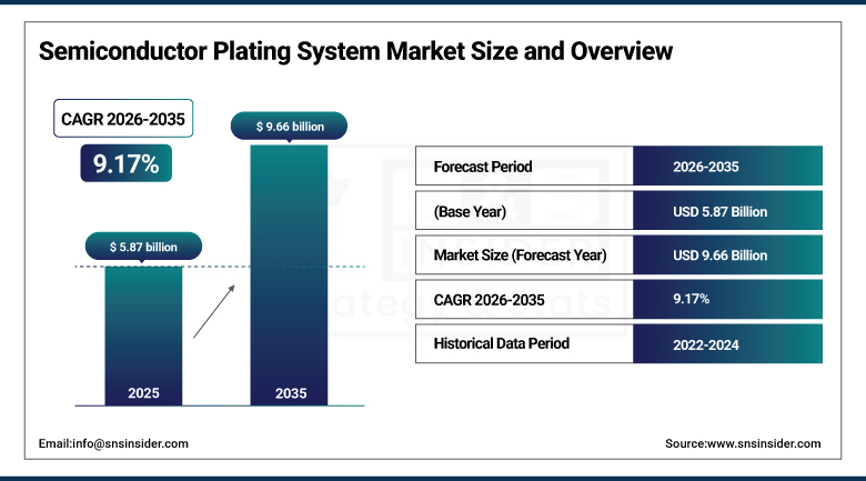
The Semiconductor Plating System Market size was valued at USD 5.87 Billion in 2025 and is expected to reach USD 9.66 Billion by 2035, growing at a CAGR of 5.12% over the forecast period of 2026-2035.
The growth of semiconductor plating system market is primarily due to EV-induced demand for precision power-management components, 5G/IoT requirements for miniaturized plating on advanced packaging, sustainability mandates promoting ecofriendly chemistries, and automation/AI-boosted efficiency and yield.
The semiconductor plating system market is also speeding up with quick foundry capacity expansion globally, which drives the demand for plating tools applied in semiconductor fabrication. The growing needs for ultra precise plating on new substrates are driven by the high-volume adoption of MEMS, sensors, optoelectronics and power devices. Growth of data centre and cloud infrastructure boost complexity of packaging applications. The automated, ultra-lean feature plating systems made possible by precision robotics, real time control, and drip-less innovations that reduce defects, waste and cost per wafer while increasing throughput.
Semiconductor Plating System market trends include rising demand for advanced interconnects in quantum computing, increasing R&D investments in hybrid substrate technologies, the shift toward localized manufacturing to reduce supply chain risks, and enhanced collaborations between equipment makers and research institutions.
Between 2023–2024, 35+ major semiconductor electroplating system upgrades launched, including sub‑7 nm copper tools achieving <20 nm line/space widths with <1.3% uniformity variance.
Semiconductor Plating System Market Size and Forecast:
-
Market Size in 2025: USD 5.87 Billion
-
Market Size by 2035: USD 9.66 Billion
-
CAGR: 5.12% from 2026 to 2035
-
Base Year: 2025
-
Forecast Period: 2026–2035
-
Historical Data: 2022–2024
To Get More Information On Semiconductor Plating System Market - Request Free Sample Report
Semiconductor Plating System Market Highlights:
-
ACM Research advances panel-level packaging technology. ACM delivered its first Ultra ECP ap‑p panel electrochemical plating tool, enabling scalable, high‑throughput copper deposition for large‑panel advanced packaging, a key milestone in the semiconductor plating equipment market
-
Industry recognition for innovation. ACM’s Ultra ECP ap‑p tool received the 2025 3D InCites Technology Enablement Award for enabling high‑volume fan‑out panel‑level packaging, reflecting strong market interest in next‑generation heterogeneous integration solutions
-
Academic and R&D expansion with advanced plating tools. Université de Sherbrooke’s Interdisciplinary Institute for Technological Innovation (3IT) installed ClassOne Technology’s Solstice® LT single‑wafer plating system, replacing manual wet benches and supporting research in AI, quantum computing, MEMS, and advanced 3D integration
-
Growing deployment of advanced plating platforms. Continued academic and industry investments in advanced plating systems, including Solstice S8 orders at research institutions like Penn State, highlight expanding demand for automated, high‑precision plating tools in both R&D and pilot applications
-
Shift toward automated and integrated plating solutions. The market is seeing a clear move from manual wet processing to automated, single‑wafer and panel‑level electroplating systems, driven by requirements for improved process control, repeatability, and support for complex advanced packaging architectures
-
Broadening applications across advanced packaging. These technology deployments and innovations support a range of advanced packaging trends, including fan‑out panel‑level packaging, TSVs, copper redistribution layers, and high‑aspect‑ratio features critical for next‑generation semiconductor devices
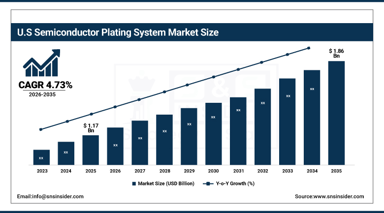
The U.S. Semiconductor Plating System Market size was valued at USD 1.17 billion in 2025 and is projected to grow at a CAGR of 4.73%, reaching USD 1.86 billion by 2035. There is a high demand for advanced chip packaging that drives growth of the U.S. semiconductor plating system market, along with the introduction of policies and incentives to spur productivity in domestic semiconductor manufacturing, intensifying technologies, such as AI and 5G, that are becoming mainstream, a robust push for automation and supply chain resilience.
Semiconductor Plating System Market Drivers:
-
Rising Demand for Advanced Semiconductor Devices Accelerates Global Adoption of Plating Systems and Packaging Technologies
Demand for advanced semiconductor devices is increasing in emerging technologies including artificial intelligence, 5G, automotive electronics, and IoT, primarily driving the global semiconductor plating system market growth. These growing requirements of high-reliability interconnects, fine-line plating and better electrical performance are driving the semiconductor industry toward a wider adoption of electroplating systems. The move toward smaller nodes and heterogeneous integration has also accelerated plating for use in advanced packaging methods, namely fan-out wafer level packaging (FOWLP) and 3D stacking. The market is also aided by government initiatives and private investments in semiconductor foundries in Asia, North America, and Europe.
In 2024, logic ICs, led by AI processors and HPC SoCs, made up nearly 38% of fan-out and interposer packaging volume underscoring plating’s critical role in high-density chiplets.
Semiconductor Plating System Market Restraints:
-
Integration Challenges and Skilled Workforce Shortage Hinder Growth of Advanced Semiconductor Plating System Market
Technical complexity and integration challenges create the significant restraints can easily be determined in the global semiconductor plating system market. Providing uniform and defect-free plating at nanoscales is getting challenging as semiconductor devices are getting smaller in geometry. Highly engineered and process-controlled advanced plating systems which enable a broad range of plating chemistries such as copper, cobalt and nickel. Also, managing so advanced systems require professionals with the right skill sets which we currently lack.
Semiconductor Plating System Market Opportunities:
-
Sustainable Plating Solutions and Smart Technologies Unlock New Growth Opportunities in Semiconductor Plating Market
From the perspective of global sustainability, there are great development opportunities for environmentally friendly plating chemistries and closed-loop plating system. The growing emphasis on automation, artificial intelligence-based process monitoring, and hybrid material plating systems creates a path for innovation. In addition, the growing global markets for data center expansion and electric vehicles are entering new domains for precision semiconductor plating solutions.
Edge-AI and virtual metrology systems are now detecting wafer defects 20% faster than manual checks and have slashed process variation by over 20% across deposition tools.
Semiconductor Plating System Market Segment Analysis:
By Application
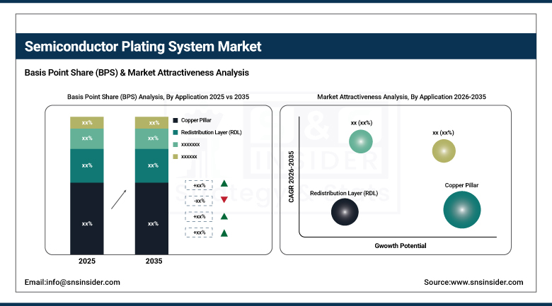
Copper pillar technology accounted for the largest share of the semiconductor plating system market in 2025, at 23.2% as it has been widely adopted due to its high electrical and thermal conductivity, high electromigration resiliency, and the ability to scale down to fine-pitch. Due to the rising need for advanced packaging to support superior performance processors and high-performance computing devices, copper pillars are widely adapted in flip-chip packaging as well as HDI (High-Density Interconnect).
Owing to its wider adoption in 3D IC packaging, memory integration, and stacked die applications, the Through-Silicon Via (TSV) technology is expected to grow at the fastest CAGR over 2026-2035. The advantages offered by TSV include shortened interconnect paths, lower power, and shorter signal path-significant benefits for AI, 5G and data-heavy applications. TSV is predicted to be much more important in the coming years since the industry is moving towards heterogeneous integration and advanced packaging.
By Technology
Electroplating held the largest share of the global semiconductor plating system market at 67.4% in 2025. The dominance of ALD is fueled by its extensive use in front-end and back-end semiconductor processes to provide excellent precise control of metal layer thickness with superior adhesion and scalability for high-volume production. Electroplating plays an important role in many applications, e.g. copper interconnects, redistribution layer (RDL), and bump formation in flip-chip packaging.
Electroless plating is estimated to have the fastest CAGR over 2026-2035. This growth is driven by rapid and uniform as the process deposits metal uniformly without requiring any outside electric current an important advantage in complex 3D surfaces and high-aspect-ratio structures. Its advantages in UBM, barrier layer formation and flexible electronics applications are fueling higher adoption for next-generation semiconductor packaging solutions.
By Wafer Size
The global semiconductor plating system market share was dominated by the above 200 mm wafer segment, which accounted for a 55.0% share in 2025. The reason for this domination comes from the dominant use of 300 mm wafers for HVM (high-volume manufacturing) in high end logic, memory and HPC (high-performance computing-based) chips. Due to superior economies of scale, higher throughput, and enhanced yield, these larger wafers are the dominant choice for leading-edge semiconductor fabs. Driven by growing demand from AI, 5G, and data center applications, the usage of above 200 mm wafers in advanced packaging and interconnect technologies continues to ramp up.
The segment of 100 mm to 200 mm wafers is projected to exhibit the quickest CAGR during the forecast period of 2026-2035. Driven by increasing demand in power electronics, MEMS, RF devices and automotive applications, smaller wafer sizes are still common thus this growth is expected. According to the company, growth was led by increased legacy node production and the expansion of specialty devices.
Semiconductor Plating System Market Regional Analysis:
Asia-Pacific Semiconductor Plating System Market Trends:
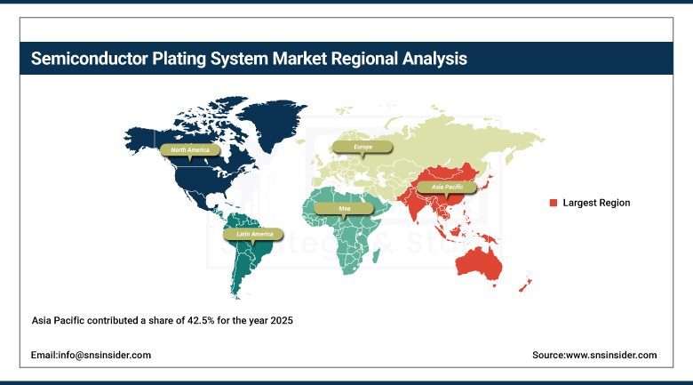
Asia Pacific contributed a share of 42.5% for the year 2024 and is anticipated to witness the fastest CAGR of 5.51% over 2026-2035. This growth is bolstered by the presence of dense semiconductor foundries, packaging and testing facilities, and investment in advanced manufacturing infrastructure. A well-developed electronics supply chain, a large, skilled labor force, and rising demand for consumer electronics, automotive semiconductors and industrial automation drive growth in the region. Further, the growing use of advanced packaging including 3D ICs, fan-out wafer-level packaging, and TSV is contributing to the demand for precision plating systems. Positive initiatives by the government, including plans to develop global fabrication hubs, and collaboration between major players in the fabrication sector, are moving the needle toward advancement and growth of the technology and fabrication capacity in the region, solidifying the region's global market leadership.
China accounted for the largest share of the Asia Pacific semiconductor plating system market, driven by massive semiconductor manufacturing investments, growing foundry capacity, increased government support, and high demand for consumer electronics and electric vehicles.
Get Customized Report as Per Your Business Requirement - Enquiry Now
The growth of semiconductor plating system market in North America is attributed to high investments in the domestic chip manufacturing sector, increasing demand for advanced packaging, and strong adoption of AI and high-performance computing in the region. New and expanding fabs are coming online in the region to bolster supply chain resiliency. Plating automation, AI-based monitoring, and environmentally sustainable processes are developed and developed more actively, which is facilitating market development as well.
North America Semiconductor Plating System Market Trends:
The North American semiconductor plating system market is led by the U.S. owing to its highly developed R&D capabilities, presence of major chip manufacturers, government funding initiatives and a major focus on domestic semiconductor production.
Europe Semiconductor Plating System Market Trends:
The Market for Semiconductor Plating System in Europe is very slowly growing due to the automotive electronics, industrial automation, and power semiconductor application segments. Region pushes to boost chip independence via state-facilitated programs and PPPs While the increasing adoption of EVs and renewable energy generation technologies fuels demand, precision plating systems are also gaining traction with many industrial companies in the semiconductor, aerospace and defense, and oil and gas sectors. The market is also witnessing growth due to technological innovation in advanced packaging as well as sustainable manufacturing.
The high level of industrialisation and the dominance in automotive applications placed Germany at the heart of the European semiconductor landscape, but also presumed to be its catalyst for semiconductor Innovation and Design (I&D) and fabrication capabilities (Fabs).
Latin America and Middle East & Africa Semiconductor Plating System Market Trends:
Latin America and Middle East & Africa (MEA) are considered as the regions of emerging semiconductor plating system market. However they are anticipated to grow at a slow pace, and the growth is expected to be on the account of growing electronics manufacturing and growing industrial digitalization in this region. Both regions are receiving large infrastructure, automotive, and energy investments, which will continue to create demand for semiconductor components.
Semiconductor Plating System Market Competitive Landscape:
Naura Technology Group Co., Ltd. Established in 2001 is a leading Chinese semiconductor equipment manufacturer specializing in plating, etching, deposition, and cleaning systems. The company serves IC fabrication, advanced packaging, and compound semiconductor markets, supporting China’s semiconductor self-reliance with strong R&D capabilities and expanding global presence.
-
In June 2025, Naura Technology has acquired control of Kingsemi, marking a strategic consolidation aimed at boosting China's domestic capabilities in advanced semiconductor lithography systems.
Applied Materials Established in 1967is a global leader in semiconductor manufacturing equipment. Its Endura Copper Barrier solution delivers advanced PVD barrier layers for copper interconnects, enabling improved reliability, reduced line resistance, and enhanced performance in advanced logic and memory device fabrication processes.
-
In April 2024, Launched the Endura Copper Barrier Seed IMS with Volta Ruthenium CVD tool to support copper wiring at 2 nm and beyond.
Semiconductor Plating System Market Key Players:
-
Applied Materials, Inc.
-
SCREEN Holdings Co., Ltd.
-
EBARA Corporation
-
ASM International N.V.
-
Kokusai Electric Corporation
-
SEMES Co., Ltd.
-
SÜSS MicroTec SE
-
NAURA Technology Group Co., Ltd.
-
Hitachi High-Tech Corporation
-
Canon Machinery Inc.
-
Veeco Instruments Inc.
-
Advantest Corporation
-
Shibaura Mechatronics Corporation
-
ULVAC, Inc.
-
Mattson Technology, Inc.
-
Besi Netherlands B.V.
-
CVD Equipment Corporation
-
Aixtron SE
| Report Attributes | Details |
|---|---|
| Market Size in 2025 | USD 5.87 Billion |
| Market Size by 2035 | USD 9.66 Billion |
| CAGR | CAGR of 5.12% From 2026 to 2035 |
| Base Year | 2025 |
| Forecast Period | 2026-2035 |
| Historical Data | 2022-2024 |
| Report Scope & Coverage | Market Size, Segments Analysis, Competitive Landscape, Regional Analysis, DROC & SWOT Analysis, Forecast Outlook |
| Key Segments | • By Application (TSV, Copper Pillar, Redistribution Layer (RDL), Under Bump Metallization (UBM), Bumping, and Others) • By Technology (Electroplating, and Electroless) • By Wafer Size (Up to 100 mm, 100 mm - 200 mm, and Above 200 mm) |
| Regional Analysis/Coverage | North America (US, Canada), Europe (Germany, UK, France, Italy, Spain, Russia, Poland, Rest of Europe), Asia Pacific (China, India, Japan, South Korea, Australia, ASEAN Countries, Rest of Asia Pacific), Middle East & Africa (UAE, Saudi Arabia, Qatar, South Africa, Rest of Middle East & Africa), Latin America (Brazil, Argentina, Mexico, Colombia, Rest of Latin America). |
| Company Profiles | Lam Research Corporation, Applied Materials Inc., Tokyo Electron Limited, SCREEN Holdings Co. Ltd., EBARA Corporation, ASM International N.V., Kokusai Electric Corporation, SEMES Co. Ltd., SÜSS MicroTec SE, NAURA Technology Group Co. Ltd., Hitachi High-Tech Corporation, Canon Machinery Inc., Veeco Instruments Inc., Advantest Corporation, Shibaura Mechatronics Corporation, ULVAC Inc., Mattson Technology Inc., Besi Netherlands B.V., CVD Equipment Corporation, and Aixtron SE. |
Frequently Asked Questions
Asia Pacific dominated the Semiconductor Plating System Market in 2025.
The Electroplating segment dominated the Semiconductor Plating System Market in 2025.
The major growth factor of the Semiconductor Plating System Market is the increasing demand for advanced packaging and miniaturized semiconductor devices requiring precise and reliable metal deposition.
The Semiconductor Plating System Market size was valued at USD 5.87 Billion in 2025 and is expected to reach USD 9.66 Billion by 2035
The Semiconductor Plating System Market is expected to grow at a CAGR of 5.12% from 2026-2035.
Get in Touch
