Wafer-level Silicon Photonic Test System Market Size Analysis:
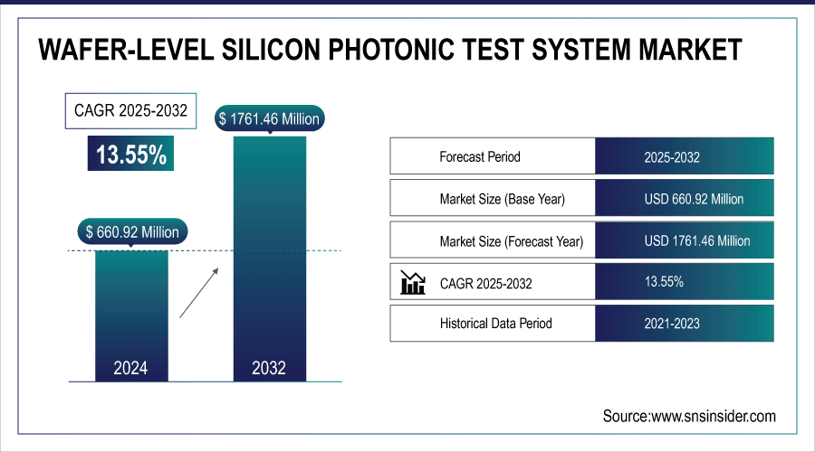
The Wafer-level Silicon Photonic Test System Market Size was valued at USD 660.92 million in 2024 and is expected to reach USD 1761.46 million by 2032 and grow at a CAGR of 13.55 % over the forecast period 2025-2032.
The worldwide wafer-level silicon photonic test system market is growing quickly on account of increasing adoption of silicon photonics technology in data centers, telecommunications and new applications such as quantum computing. The growing popularity of wafer-level test systems can be attributed to advances in automatic test equipment, combined with growing investment in the research and development of photonics which are supporting higher precision, throughput and economies of scale in the manufacture of photonic devices.
According to research, Adoption of wafer-level photonic test systems has enabled cost savings of up to 30% per device in production lines.
To Get More Information On Wafer-level Silicon Photonic Test System Market - Request Free Sample Report
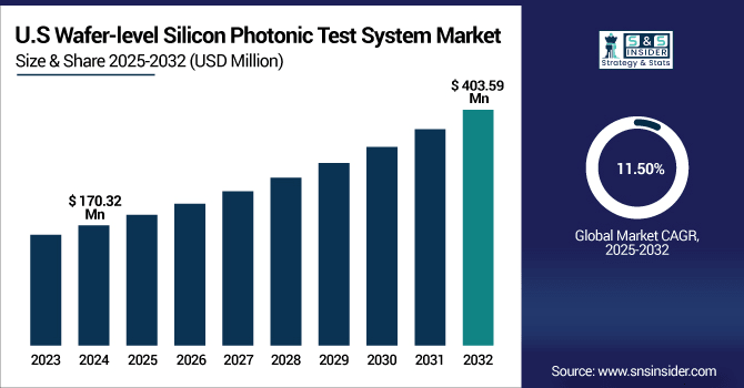
The U.S. Wafer-level Silicon Photonic Test System Market size was USD 170.32 million in 2024 and is expected to reach USD 403.59 million by 2032, growing at a CAGR of 11.50 % over the forecast period of 2025–2032.
The U.S. Wafer-level Silicon Photonic Test System Market growth is attributed the development of high-technology and surging investments in silicon photonics by government and private sector. Growth of data center industry and increasing demand for faster and efficient communication systems are more supportive to the demand. In addition, the existence of world-class test equipment vendors and R&D centers drives wafer-level test solutions adoption.
Wafer-level Silicon Photonic Test System Market Dynamics
Key Drivers:
-
Rising Adoption of Automated Testing Systems in Semiconductor Manufacturing Accelerates Market Expansion
It improves wafer-level Photonics testing throughput, minimizes the error, and lowers operation costs. With the increasing silicon photonic wafer production volume and complexity, manufacturers are turning to automated test solutions. This transition to automated systems enables high efficiency and rapid scalability in production test environments, and adds to the growing wafer-level silicon photonic test system market around the globe. Moreover, automation supports the real-time data analyses and quality control, promoting the faster process for decision making which helps to decrease the time span for market launches of advanced photonic devices.
According to research, Automated testing solutions can improve wafer-level photonics testing throughput by up to 40–50% compared to manual or semi-automated processes.
Restrain:
-
Lack of Standardized Testing Protocols and Industry Fragmentation Hinder Market Adoption
Lack of standard techniques for testing silicon photonics devices leads to inconsistency in testing approaches. Focus on component coupling and package technology leads to fragmentation amongst tools providers and manufacturers limitation or stop of large scale implementation of wafer level test systems. The absence of standards impedes the penetration of the market and delays the adoption in different regions and areas. And it adds to the costs and complexity for end users who must customize or modify testing procedures, which restricts efficiency and retards innovation in the silicon photonic test ecosystem globally.
Opportunities:
-
Growing Applications in Data Centers and Telecom Create New Market Opportunities
Growing applications of silicon photonics for high bandwidth and low latency communications in data center and telecommunications infrastructure are creating additional opportunities for wafer-level test system adoption. Growing requirements for energy-saving optical interconnects are driving constant innovation and demand for advanced test solutions, which is lucrative for market participants to capitalize on new areas. Moreover, the exponential growth in cloud computing, 5G network deployments, edge computing applications is boosting the need for robust and scalable photonic testing technologies and accelerating the market growth across the globe.
According to research, Optical interconnects can reduce data center energy consumption by up to 30% compared to traditional copper-based solutions, driving adoption.
Challenges:
-
Rapid Technological Evolution Requires Continuous Upgradation of Test Systems, Posing Market Challenges
The rapid advancement of silicon photonics technology requires frequent release and calibration of test equipment that will increase maintenance complexity and cost. This fast evolution is putting pressure on producers to stay up-to-date with the new device architectures, impeding the operation and hindering some users from performing WLT using the test systems. Additionally, the ongoing requirement for software and hardware updates can deplete resources, especially for small manufactures, branding them unable to take full advantage of the latest technologies and resulting in a reduction of market growth and technology dissemination.
Wafer-level Silicon Photonic Test System Market Segment Analysis:
By Type
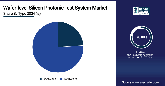
Hardware segment dominated the highest Wafer-level Silicon Photonic Test System Market share of about 76.00% in 2024 because of its importance for high-precision measurement and performance verification of photonic chips. A hardware solution that is robust and accurate is required due to increased complexity and shrinking size of photonic integrated circuits. A company such as FormFactor Inc. has been a major player in pushing hardware forward, providing a scalable solution that dovetails with today's production. Their solutions are high-throughput capable, hence making a hardware essential in today's production of wafer-level silicon photonics.
Software segment is expected to grow at the fastest CAGR of about 14.79% from 2025–2032, due to the increasing requirement for intelligent data processing, test automation, and real-time analytics in photonic test systems. Software is becoming more and more important for addressing challenging device structures and for maximizing test efficiency. Wafer-level Silicon Photonic Test System Companies including AEM Holdings Ltd. are developing software platforms that combine machine learning and cloud functionality, enhancing flexibility of test systems for faster responses to design iterations, underpinning the software segment's growth.
By Application
300mm Wafer segment dominated the Wafer-level Silicon Photonic Test System Market with the highest revenue share of about 37.20% in 2024, because it is used in many semiconductor advanced manufacturing processes, as well as mass production for photonics. The cost-effectiveness of 300mm wafers and their size, makes them the largest wafer size for data centers and high-speed networking. Companies such as Intel Corporation are leading this segment, as development of silicon photonics on 300mm wafers becomes more pervasive, which, combined with large-scale fabrication and integrated testing infrastructure, firmly establishes this segment's dominance.
200mm Wafer segment is expected to grow at the fastest CAGR of about 14.14% from 2025–2032, fueled by its use in prototyping, research laboratories and niche photonics applications in which flexibility and low-cost manufacturing provide advantages. A proliferating interest in integrated photonics from both academia and startups is fueling its expansion. Vanguard International Semiconductor Corporation is one such firm using 200mm wafer platforms to design future photonic devices and is driving the segment’s growth at a rapid velocity.
Wafer-level Silicon Photonic Test System Market Regional Outlook:
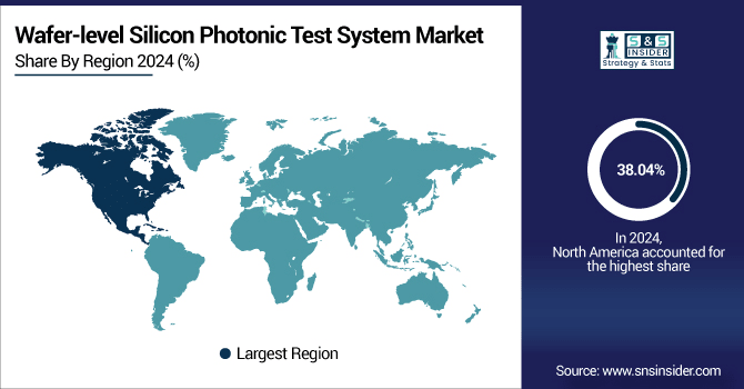
North America dominated the Wafer-level Silicon Photonic Test System Market with the highest revenue share of about 38.04% in 2024 because of the strong participation of leading photonics companies, an advanced semiconductor R&D infrastructure, and a large investment from the government and industry for optical communication technologies. The U.S. is one of the leading data center and telecom innovation centers and has a growing need for advanced silicon photonic test systems. Powerful partnerships between universities and technology companies also fuel constant innovation and a leading market position in this region.
Get Customized Report as Per Your Business Requirement - Enquiry Now
-
The U.S. holds the largest share in the North American wafer-level silicon photonic test system market due to its advanced semiconductor infrastructure, strong R&D environment and availability for major photonics companies and the presence of the demand from data centers and the telecom industry for innovation and testing capabilities.
Asia Pacific is expected to grow at the fastest CAGR of about 14.29% from 2025–2032, driven by increasing semiconductor production, growing 5G deployment and increasing acceptance of silicon photonics in developing nations such as China, Japan and South Korea. Photonics initiatives in the government and massive investments in optical communication networks are the driving forces behind this market’s growth. Moreover, the rise of local foundries and test equipment providers support access to and the affordability of wafer-level silicon photonic testing solutions driving Asia pacific as a burgeoning market for wafer-level silicon photonic testing offerings.
-
China is dominated in the Asia Pacific wafer-level silicon photonic test system market on account of its significant semiconductor manufacturing capabilities, favourable support from the government, expanded of 5G infrastructure, and growing investments in photonics R&D, which has resulted in increased domestic demand for test solutions and technology innovations.
Wafer-level Silicon Photonic Test System Market in Europe, led by support from photonics research, robust industry-academia associations across subcontinent, and the existence of large number of prominent companies exploring potential in semiconductor and telecommunication sector. Information Countries such as Germany, the Netherlands and France are investing in photonics and quantum technologies, promoting innovation. Precision engineering and sustainability are highlighted in the region, conducive to market expansion and global competitiveness.
-
Germany leads the European Wafer-level Silicon Photonic Test System Market owing to its strong semiconductor industry backed by the top R&D facilities and being a pioneer in the photonics technology development. Its strong manufacturing ecosystem, coupled with R&D and industry initiatives, presents a robust technology supply chain for gaining an increasing share of the market.
The market in the Middle East & Africa (MEA) and Latin America for wafer-level silicon photonic test systems is expected to grow significantly in the coming years. Nations such as the UAE, Saudi Arabia and Brazil are boosting the demand with investments in telecommunication, data centers and smart technology projects and the investments have opened new opportunities for advanced photonic testing solutions.
Wafer-level Silicon Photonic Test System Companies are:
Major Key Players in Wafer-level Silicon Photonic Test System Market are Advantest Corporation, Teradyne Inc., FormFactor Inc., Hangzhou Changchuan Technology Co., Ltd., Keysight Technologies, MPI Corporation, Fiberpro Inc., SemiProbe Inc., Aerotech Inc., Physik Instrumente (PI) GmbH & Co. KG and others.
Recent Development:
-
In March 2025, Teradyne announced a production system for double-sided wafer probe testing for silicon photonics. This development aims to enhance testing efficiency and precision in the growing field of silicon photonics.
-
In December 2023, MPI Corporation introduced the MP1200 Probe Station, a high-precision wafer probe system optimized for testing silicon photonic devices.
| Report Attributes | Details |
|---|---|
| Market Size in 2024 | USD 660.92 Million |
| Market Size by 2032 | USD 1761.46 Million |
| CAGR | CAGR of 13.15% From 2025 to 2032 |
| Base Year | 2024 |
| Forecast Period | 2025-2032 |
| Historical Data | 2021-2023 |
| Report Scope & Coverage | Market Size, Segments Analysis, Competitive Landscape, Regional Analysis, DROC & SWOT Analysis, Forecast Outlook |
| Key Segments | • By Type (Software, Hardware) • By Application (300mm Wafer, 200mm Wafer, 150mm Wafer, Others) |
| Regional Analysis/Coverage | North America (US, Canada, Mexico), Europe (Germany, France, UK, Italy, Spain, Poland, Turkey, Rest of Europe), Asia Pacific (China, India, Japan, South Korea, Singapore, Australia,Taiwan, Rest of Asia Pacific), Middle East & Africa (UAE, Saudi Arabia, Qatar, South Africa, Rest of Middle East & Africa), Latin America (Brazil, Argentina, Rest of Latin America) |
| Company Profiles | Advantest Corporation, Teradyne Inc., FormFactor Inc., Hangzhou Changchuan Technology Co., Ltd., Keysight Technologies, MPI Corporation, Fiberpro Inc., SemiProbe Inc., Aerotech Inc., Physik Instrumente (PI) GmbH & Co. KG. |
Frequently Asked Questions
Ans: North America dominated the Wafer-level Silicon Photonic Test System Market in 2024.
Ans: Hardware segment dominated the Wafer-level Silicon Photonic Test System Market.
Ans: The major growth factor of the Wafer-level Silicon Photonic Test System Market is the increasing adoption of silicon photonics in data centers and telecommunications, boosting demand for advanced testing systems.
Ans: The Wafer-level Silicon Photonic Test System Market size was USD 660.92 million in 2024 and is expected to reach USD 1761.46 million by 2032.
Ans: The Wafer-level Silicon Photonic Test System Market is expected to grow at a CAGR of 13.15 % from 2025-2032.
Get in Touch
