The global semiconductor teardown services market will experience growth due to increasing investments made by semiconductor manufacturers, electronics firms and intellectual property organizations into analysis, reverse engineering and benchmarking of their components. Increased complexity of semiconductors, sophisticated semiconductor packaging and issues related to counterfeit components have created the need for specialized teardown facilities.
As per reports from SNS Insider, the global semiconductor teardown services market reached the value of USD 1.53 billion in 2025, is estimated to be worth USD 1.64 billion in 2026 and further expected to grow to USD 3.13 billion by 2035, at a CAGR of 7.43% between 2026 and 2035.
Semiconductor teardown services involve systematically examining integrated circuits, electronic components and finished devices to identify internal architectures, manufacturing technologies, material composition and circuit configurations. They offer assistance in competitive intelligence, patent research, vendor validation, and product development.
The rising use of artificial intelligence processors, packaging, computing chips, and complicated consumer electronics is generating more analysis needs. There is a greater need for information about competing products to assess their capabilities and innovations in design.
North America continues to be the biggest market region, whereas Asia-Pacific is anticipated to grow the fastest until 2035.
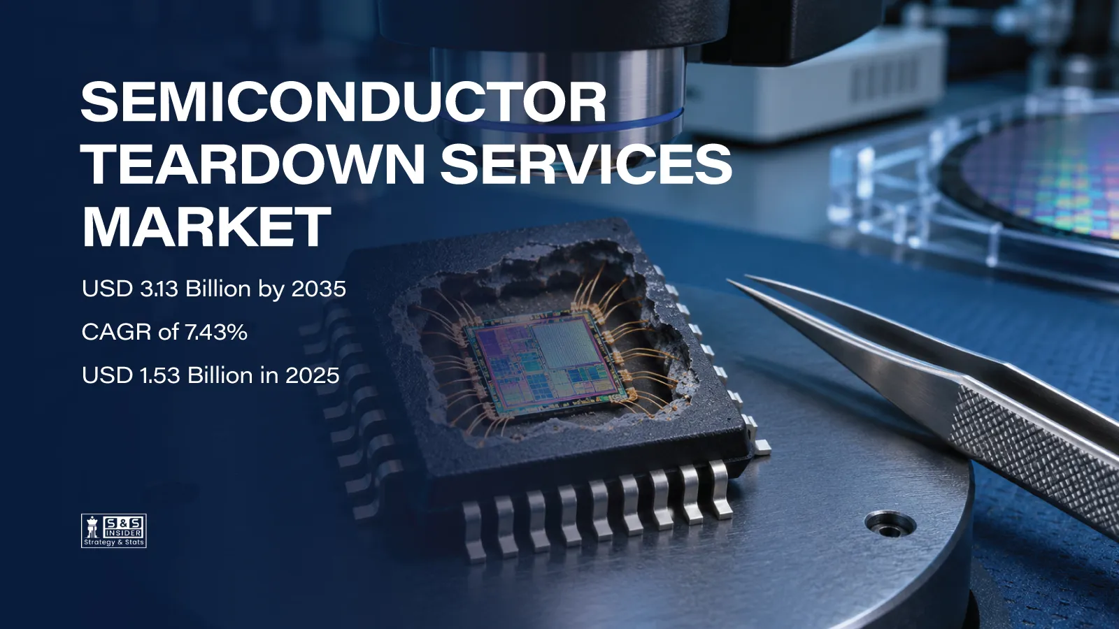
Semiconductor Teardown Services Market Size and Forecast
|
Market Indicator |
Value |
|---|---|
|
Market Size, 2025 |
USD 1.53 Billion |
|
Market Size, 2026 |
USD 1.64 Billion |
|
Market Forecast, 2035 |
USD 3.13 Billion |
|
CAGR, 2026–2035 |
7.43% |
|
North America Market Share, 2025 |
38.92% |
|
Asia-Pacific Forecast CAGR |
8.55% |
|
Leading Application |
Circuit Extraction & Reverse Engineering |
|
Leading Device Type |
Smartphones & Laptops |
Demand Drivers and Constraints
Primary Demand Drivers
-
Increasing semiconductor complexity: Advanced process nodes, chiplet architectures and multilayer packaging technologies require sophisticated imaging and physical analysis capabilities.
-
Rising intellectual property disputes: Semiconductor companies use teardown analysis to investigate potential patent infringement and evaluate competing circuit designs.
-
Growing counterfeit component concerns: Automotive, defense and industrial electronics manufacturers increasingly require component authentication and semiconductor supply chain verification.
-
Expansion of competitive benchmarking: Electronics manufacturers analyze competing processors, memory devices and integrated circuits to understand technological differences.
-
Growing semiconductor innovation: Investments in artificial intelligence, advanced computing, automotive electronics and communication technologies are increasing demand for independent technical assessments.
-
Advancements in analytical equipment: Improvements in electron microscopy, focused ion beam systems and automated imaging technologies enable more detailed semiconductor examination.
Potential Growth Constraints
-
High acquisition and maintenance costs for advanced semiconductor analysis equipment.
-
Shortages of engineers experienced in circuit extraction, failure analysis and chip reverse engineering.
-
Export restrictions and intellectual property regulations affecting sensitive semiconductor technologies.
-
Increasing difficulty analyzing advanced packaging structures and security-protected integrated circuits.
-
Extended project timelines for complex semiconductor devices requiring multilayer imaging and detailed circuit reconstruction.
Demand Structure by Method
Force Flow (Energy Flow Field) — 45.71% Market Share in 2025
Force flow represents the leading semiconductor teardown methodology, accounting for approximately 45.71% of global market revenue in 2025.
It helps in analyzing semiconductors by utilizing methods which use energy analysis. This method is especially applicable in labs that are trying to analyze advanced chips and semiconductors.
There is increasing need for advanced imaging systems due to the growing trend of miniaturization in the field of semiconductors.
Current trend: Expanding use of advanced physical analysis techniques for semiconductor structure characterization.
Major trends: Electron microscopy, internal structure mapping, high-resolution imaging and advanced package inspection.
Measurement & Experimentation — 8.17% Forecast CAGR
Measurement and experimentation is projected to register the fastest growth among methods, expanding at a CAGR of approximately 8.17% during 2026–2035.
Demand is rising since semiconductor makers need to conduct thorough tests on their electrical, thermal, and functional performances along with physical inspections.
Testing services assist engineers in evaluating the component performance, comparing different technologies, and studying the reliability of devices. The rise in power semiconductors, sensors and high-performance ICs is fueling demand for testing services.
Current trend: Increasing integration of electrical testing with semiconductor teardown investigations.
Major trends: Functional characterization, thermal testing, precision measurement and integrated laboratory analysis.
Demand Structure by Application
Circuit Extraction & Reverse Engineering — 40.26% Market Share in 2025
Circuit extraction and reverse engineering dominate the application segment, holding approximately 40.26% of the global market in 2025.
Semiconductor companies and intellectual property experts make use of these services to conduct an investigation of circuit designs and manufacturing process of competitors.
Reverse engineering is the process of studying the semiconductor layers and deriving relevant information on circuits for comparison and patenting purposes.
The rise in investments in advanced processors, artificial intelligence accelerators, and memory technology has resulted in rising demand for circuit analysis.
Current trend: Strong demand for semiconductor architecture evaluation and patent-related technical investigations.
Major trends: Circuit reconstruction, semiconductor patent analysis, advanced-node examination and competitive benchmarking.
Counterfeit Screening Database — 9.34% Forecast CAGR
Counterfeit screening database applications are expected to record the fastest growth, with a CAGR of approximately 9.34% during 2026–2035.
Increasing concerns regarding counterfeit, altered and unauthorized semiconductor components are encouraging electronics manufacturers to strengthen component verification procedures.
Specialized laboratories use imaging, electrical inspection and physical authentication to identify inconsistencies between genuine and potentially counterfeit devices.
Automotive, aerospace, defense and industrial electronics manufacturers represent important demand sources because component authenticity directly affects product reliability.
Current trend: Increasing adoption of semiconductor authentication and traceability solutions.
Major trends: Component verification databases, counterfeit detection, automated image comparison and supply chain security.
Demand Structure by Device Type
Smartphones & Laptops — 33.47% Share and 8.91% Forecast CAGR
Smartphones and laptops represent the largest device segment, accounting for approximately 33.47% of the global semiconductor teardown services market in 2025.
The segment is also projected to grow at a CAGR of 8.91% during 2026–2035.
Modern smartphones and laptops integrate advanced processors, memory chips, wireless communication components, sensors and sophisticated power management systems.
Frequent product launches and intense competition encourage manufacturers to investigate competing devices and identify improvements in semiconductor architecture.
Increasing adoption of on-device artificial intelligence, advanced mobile processors and energy-efficient computing technologies is creating additional requirements for detailed device analysis.
Current trend: Increasing semiconductor benchmarking associated with next-generation smartphones and AI-enabled laptops.
Major trends: Processor architecture analysis, advanced memory inspection, AI chip evaluation and component-level competitive intelligence.
Demand Structure by End User
Consumer Electronics — 38.15% Market Share in 2025
Consumer electronics represent the largest end-user segment, accounting for approximately 38.15% of global revenue in 2025.
Manufacturers of smartphones, televisions, wearable electronics and connected devices rely on teardown services to evaluate competing technologies, identify semiconductor suppliers and understand product design decisions.
Rapid product replacement cycles and growing demand for advanced functionality encourage manufacturers to maintain comprehensive competitive intelligence programs.
The increasing integration of sophisticated semiconductor components across consumer products supports recurring demand for technical analysis.
Current trend: Growing use of independent semiconductor analysis in consumer electronics product development.
IT & Telecommunications — 8.62% Forecast CAGR
IT and telecommunications is projected to be the fastest-growing end-user segment, expanding at a CAGR of approximately 8.62% from 2026 to 2035.
Demand is supported by developments in data center processors, telecommunications infrastructure, networking equipment and artificial intelligence accelerators.
Technology companies increasingly require detailed semiconductor analysis to evaluate competing computing architectures and validate component capabilities.
Current trend: Rising demand for analysis of networking semiconductors, custom accelerators and advanced computing devices.
Regional Market Dynamics
North America — 38.92% Market Share in 2025
North America dominates the global semiconductor teardown services market, supported by its established semiconductor design ecosystem, intellectual property enforcement activities and demand for advanced electronics analysis.
The United States semiconductor teardown services market was valued at USD 514.91 million in 2025 and is projected to expand at a CAGR of 7.12% during 2026–2035.
Demand comes from semiconductor manufacturers, technology companies, legal specialists, automotive suppliers and government organizations requiring detailed component analysis.
Investments in domestic semiconductor manufacturing and advanced packaging capabilities are also expected to strengthen demand for independent technical assessment.
Direction: Continued leadership supported by patent investigations, semiconductor innovation and supply chain security requirements.
Europe — Advanced Electronics and Patent Analysis Drive Demand
Europe represents an established market for semiconductor teardown services, particularly across Germany, France, the United Kingdom and the Netherlands.
The region benefits from advanced automotive electronics manufacturing, industrial semiconductor applications and research institutions specializing in microelectronics.
Demand is supported by component authentication, patent-related investigations and evaluation of sophisticated semiconductor technologies.
Direction: Steady expansion supported by automotive electronics, research capabilities and regulatory requirements.
Asia-Pacific — Fastest-Growing Region at 8.55% CAGR
Asia-Pacific is forecast to record the fastest regional growth, expanding at a CAGR of approximately 8.55% during 2026–2035.
China, Japan, South Korea, Taiwan and India represent important semiconductor manufacturing and electronics development centers.
Increasing investments in semiconductor fabrication, advanced packaging, consumer electronics and artificial intelligence hardware are creating opportunities for teardown laboratories.
Regional manufacturers are increasingly using competitive benchmarking and physical component inspection to evaluate technologies and strengthen product development.
Direction: Accelerating demand supported by semiconductor manufacturing expansion and technological competition.
Latin America and Middle East & Africa
Latin America and the Middle East & Africa represent smaller but developing markets for semiconductor teardown services.
Brazil and Mexico benefit from electronics manufacturing and automotive supply chain activities, while Gulf countries are increasing investments in advanced technology infrastructure.
Demand is expected to strengthen as local electronics industries expand and organizations place greater emphasis on component authenticity and technical verification.
Direction: Gradual market development supported by industrial modernization and electronics supply chain investments.
Competitive Landscape
The global semiconductor teardown services market includes specialized reverse engineering laboratories, semiconductor analysis companies and intellectual property consulting providers.
Major participants identified in the SNS Insider report include TechInsights, Texplained, Sagacious Research, UnitedLex, Eurofins EAG Laboratories and Lumenci.
These companies compete through analytical expertise, imaging capabilities, circuit reconstruction techniques, technical documentation quality and project delivery efficiency.
Increasing semiconductor complexity is encouraging service providers to invest in advanced microscopy, automated analysis software and specialized engineering capabilities.
Market Outlook (2026–2035)
The global semiconductor teardown services market is projected to increase from USD 1.64 billion in 2026 to USD 3.13 billion by 2035, registering a CAGR of 7.43%.
Growth will be supported by increasingly complex semiconductor architectures, intellectual property investigations, competitive benchmarking and counterfeit component detection.
Advanced packaging technologies, artificial intelligence processors and sophisticated integrated circuits will require deeper technical examinations, encouraging laboratories to improve analytical capabilities.
Demand for semiconductor authentication is also expected to expand as electronics manufacturers strengthen supplier verification and product reliability programs.
North America is expected to maintain its leading position, while Asia-Pacific offers the fastest regional growth opportunities.
Overall, the semiconductor teardown services market is positioned for sustained expansion through 2035, with competitive advantage increasingly determined by analytical precision, advanced imaging capabilities, semiconductor expertise and the ability to deliver reliable technical intelligence.