ALD Equipment Market Size & Industry Analysis:
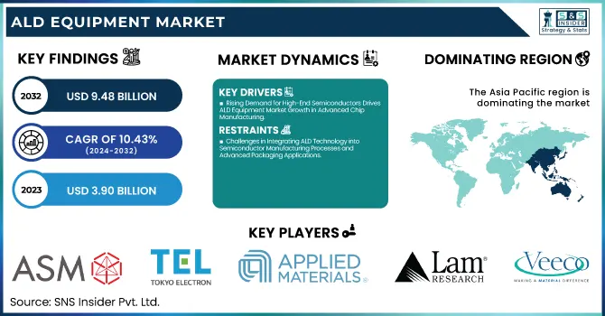
The ALD Equipment Market Size was valued at USD 3.90 Billion in 2023 and is expected to reach USD 9.48 Billion by 2032 and grow at a CAGR of 10.43% over the forecast period 2024-2032.
The Atomic Layer Deposition Equipment market is driven by Chip design trends used in Advanced 3D Architectures at sub-5nm nodes requiring precision thin film deposition. Because of the increasing demand for chip production capacity, high fab capacity utilization is pulling investments to assist in the ALD tools supply chain, whereas with higher technology nodes more profuse adoption is required to support advanced chip technologies.
Market Size and Forecast:
-
Market Size in 2023: USD 3.90 Billion
-
Market Size by 2032: USD 9.48 Billion
-
CAGR: 10.43% from 2024 to 2032
-
Base Year: 2023
-
Forecast Period: 2024–2032
-
Historical Data: 2020–2022
To Get more information on ALD Equipment Market - Request Free Sample Report
In addition, ALD, which is needed for its conformal depositions on layers that are increasingly complex multi-layer structures, also continues to see new applications arising from 3D NAND and DRAM scaling, points out the analyst. More than 500 atomic layer deposition (ALD) systems will be brought online at U.S. semiconductor fabs in 2024 alone from the combination of new technology, lots of investment in logic, DRAM, and 3D NAND production. Thus, with 12% growth in R&D budgets, U.S. companies are ramping up their research into new materials and chip designs, generating even more competition for ALD.
ALD Equipment Market Trends:
-
Rising demand for advanced semiconductor devices and miniaturized electronic components is significantly driving adoption of atomic layer deposition (ALD) systems.
-
Growing investments in foundries and chip manufacturing facilities are accelerating procurement of high-precision thin-film deposition equipment.
-
Expanding applications in memory, logic devices, and advanced packaging technologies are boosting market growth.
-
Increasing use of ALD technology in solar cells, LEDs, and power electronics is broadening industry adoption beyond semiconductors.
-
Technological advancements such as plasma-enhanced ALD (PEALD) and spatial ALD are improving deposition efficiency and scalability.
-
Strategic collaborations between semiconductor manufacturers, research institutes, and equipment providers are strengthening innovation and global market expansion.
The U.S. ALD Equipment Market is estimated to be USD 0.69 Billion in 2023 and is projected to grow at a CAGR of 10.40%. U.S. ALD Equipment Market is increasing owing to high demand for advanced semiconductor nodes, 3D packaging, and miniaturization of chips. The rising need for accurate, high-performance deposition techniques such as ALD is further triggered by the widespread adoption of energy-efficient technologies in AI, automotive, and consumer electronics sectors.
Atomic Layer Deposition (ALD) Equipment Market Drivers:
-
Rising Demand for High-End Semiconductors Drives ALD Equipment Market Growth in Advanced Chip Manufacturing
Strong demand for high-end semiconductors for computing, consumer electronics, and data center applications is the primary driver propelling the growth of the ALD (Atomic Layer Deposition) equipment market. ALD will be critical to enable next-generation nodes (5nm, 3nm, and beyond) as transistor scaling reaches its physical limits through the deposition of ultra-thin, conformal films with atomic-level precision. Further, the integration of 3D architectures into NAND and FinFETs into logic ICs has deepened the relevance of ALD technology for advanced chip manufacturing. The increasing investments in the expansion of foundries across the Asia Pacific, the U.S. CHIPS Act, and the Europe semiconductor push are propelling the deployment of high-performance ALD tools. Demand is also boosted by the use of the technology in new applications including MEMS, sensors, and quantum computing.
Atomic Layer Deposition (ALD) Equipment Market Restrain:
-
Challenges in Integrating ALD Technology into Semiconductor Manufacturing Processes and Advanced Packaging Applications
The complexity of integration into existing semiconductor manufacturing processes represents one of the major challenges in the ALD equipment market. The inability to design this technique across many other device architectures without significant process development is due to the extreme process windows and conditions such as temperature, precursor chemistry, and deposition conditions that need to be controlled in ALD. This is especially difficult in the case of heterogeneous integration and advanced packaging where interaction with multiple materials and structures is involved. Moreover, due to the low availability and volatility of some precursors for the deposition of some specific films like sulfides or fluorides, which have found increasing interest in new applications, film deposition is also limited.
Atomic Layer Deposition (ALD) Equipment Market Opportunity:
-
ALD Technology Expands into New Industries Driving Opportunities in Automotive Healthcare Energy and Power Sectors
In the presence of ALD scaling up into other applications beyond conventional semiconductors, more opportunities are opening up too. The transition towards electric vehicles (EV) within the automotive industry, in turn, opens new markets for ALD in power electronics and use in battery interfaces. ALD is also being investigated for application in the healthcare and biomedical industry for biocompatible coatings and micro/nanodevices. In addition, ALD is being used by the energy & power sector for solid-state batteries, photovoltaics, and protective coatings in severe environments. We also see the advancement in plasma-enhanced and spatial ALD systems, enabling new materials possibilities and broadening the range of industries to which the technology can be applied.
Atomic Layer Deposition (ALD) Equipment Market Challenges:
-
Challenges in ALD Deposition Rate Uniformity Environmental Concerns and Skilled Workforce Requirements for High-Volume Manufacturing
A slower deposition rate of ALD is another important bottleneck that may restrict the throughput if one considers high-volume manufacturing. Although innovations such as spatial and plasma-enhanced ALD are aiming at overcoming this, they bring their specific technical challenges including controlling uniformity across large substrates. Additionally, the regulatory and environmental concerns associated with the safe handling and disposal of chemical precursors (some of which are toxic or reactive), further complicate the operational paradigm in which manufacturers must operate. Most importantly, one challenge remains the supervision of high-level people who have to develop and refine ALD processes in diverse applications, which will be more prominent as high demand in new fields such as medical instruments and energy storage emerges.
Atomic Layer Deposition Equipment Market Segmentation Outlook
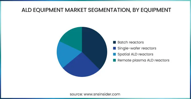
By Equipment
Batch reactors accounted for 37.5% of the ALD equipment market share in 2023. The reason behind their popularity is that they can process multiple wafers in parallel, which is extremely useful for high-throughput applications like memory device fabrication. Batch reactors are established tools in the semiconductor manufacturing world where a reasonable amount of batch processing is required to be performed on semiconductor material to produce uniform films on many wafers in parallel.
Single-wafer reactors are anticipated to register the fastest CAGR from 2024 to 2032. The increase is based on the compounded rise in demand for advanced node technologies in logic and high-performance computing applications. A key difference between single-wafer and batch reactors is that single-wafer reactors deliver a much higher degree of control of the associated film uniformity and thickness, which is critical in the manufacture of complex 3D structures and highly scaled devices.
By Deposition Method
The thermal ALD holds the largest market share of 41.3% in the year 2023. The widespread use of this tool for semiconductor manufacturing and oxide films deposited on memory devices and logic chips are the main reasons for this dominance. Well, thermal ALD is favorable because of its simplicity, high-quality film deposition, and kinematics for producing conformal films with uniform compositions across large areas (with lower temperature deposition). For many traditional applications, they remain the preferred option, delivering reliability and scalability in high-volume manufacturing.
Growth of plasma-enhanced ALD (PEALD) is expected to be the fastest among all technologies, in terms of CAGR, from 2024 to 2032. However, PEALD also has some advantages over thermal ALD, such as the low-temperature deposition ability, that is required for advanced applications including high-k dielectrics, 3D NAND, as well as more complex microelectronic structures. PEALD has emerged as an important technology for next-generation semiconductor manufacturing because it allows finer control over film properties, including higher density and lower film uniformity, thus, enabling the manufacture of smaller and more complex semiconductor devices.
By Film Type
Oxide films accounted for 39.5% of the ALD equipment market in 2023. This filled in many gaps as CMOS forms the basis of most semiconductor manufacturing processes, especially for gate oxides, passivation layers, and dielectrics. In the context of device scaling, oxide films, e.g. alumina (Al₂O₃) and hafnia (HfO₂), play a critical role on account of their thermodynamic stability, ideal electrical properties, and good thermal stability and conformality, which are applicable in fields ranging from memory devices, logic circuits to advanced packaging.
The nitride films are anticipated to witness rapid growth CAGR in this period from 2024 – 2032 years. The growing need for nitride films, particularly titanium nitride (TiN) and silicon nitride (Si₃N₄) as diffusion barriers, hard masks, and materials for advanced transistors and high-performance logic devices, woven over the activated carbon fiberfrabic or woven carbon nanofiber substrates. The high stability of nitride films, combined with excellent low leakage and high durability at high temperatures, makes them an indispensable component in next-generation semiconductors as the semiconductor industry moves to smaller nodes and higher complexities of 3D structures, rapidly increasing the demand for nitride films in the market.
By Application
The ALD equipment market was dominated by the computing sector in 2023, which represented 30.4% This dominance is propelled by the growing need for high-end processors, GPUs, and memory chips utilized in servers, personal computers, and AI/ML solutions. ALD is a key technology supporting advanced logic nodes and 3D structures needed for faster, smaller, and more efficient computing hardware. This trend has made the sector üksest the biggest status of ALD tech as the sector remains new for more innovation and scale.
The consumer electronics segment is expected to grow at the highest CAGR between the periods of 2024 and 2032. The increasing demand for smartphones, wearables, AR/VR headsets, and smart home systems has led to the growth of devices as they evolve regularly and require high-performing, compact, and energy-efficient semiconductor components. Provides the accuracy and capability of depositing conformal films of atomic-scale thickness, significant for meeting design and performance requirements for modern consumer devices, and thus establishing itself as the ubiquitous choice for this segment.
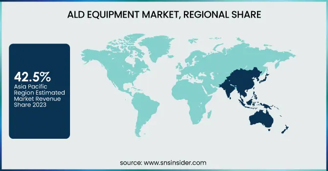
ALD Equipment Regional Analysis
In 2023, 42.5% of the ALD equipment market was attributed to Asia Pacific, capitalizing on the region’s monopoly in the global semiconductor industry. Locations such as Taiwan, South Korea, Japan, and China are where top foundries and leading-edge chipmakers such as TSMC, Samsung, and SMIC reside invest heavily in state-of-the-art deposition processes like ALD for building advanced memory and logic chips. Resize of TSMC advance nodes (5nm and 3nm) that are strongly dependent on ALD tools to deposit material layers with precision for FinFET and GAA transistor architecture. This further enhances the collaboration with the local supply chains and regular upgrades and technology advancement with government support establishing Asia Pacific to lead the world order in the global ALD market.
North America is projected to experience the fastest growth from 2024 to 2032 owing to rising investment in domestic semiconductor production. The launching of new fabs has been sped up by the U.S. CHIPS and Science Act and some companies including Intel and GlobalFoundries are planning to enhance the acquisition of advanced ALD tools for their logic and packaging needs. The recent announcement of a high-precision line dedicated to the Intel fab project in Ohio is a good example of how much the needs of next-generation chips enable ALD tools. America emerges as a new growth accelerator for ALD technology deployments driven by supply chain resilience, innovation, and AI-based demand.
Get Customized Report as per Your Business Requirement - Enquiry Now
Key Players Listed in the Atomic Layer Deposition (ALD) Equipment are:
-
ASM International (Pulsar 3000)
-
Tokyo Electron Limited (Trias Series)
-
Applied Materials, Inc. (OlympusALD)
-
Lam Research Corporation (ALTUS ALD)
-
Veeco Instruments Inc. (Savannah ALD)
-
Beneq (Beneq TFS 200)
-
Picosun (Picosun R-200 Advanced)
-
Oxford Instruments (FlexAL)
-
Kurt J. Lesker Company (ALD150LX)
-
CVD Equipment Corporation (SDS ALD System)
-
Forge Nano (Prometheus ALD)
-
Encapsulix (Infinity ALD)
-
Ultratech (Division of Veeco) (ALD Lambda)
-
SENTECH Instruments (ALD Real Time Thickness Control)
-
SÜSS MicroTec (SUSS ALD Cluster)
ALD Equipment Market Trends
-
In November 2024, Applied Materials unveiled a new collaboration model at the Summit on Energy-Efficient Computing to accelerate advanced chip packaging. The initiative expands its EPIC platform to fast-track the commercialization of energy-efficient technologies for AI and next-gen computing.
-
In February 2025, Lam Research launched the ALTUS Halo, the industry's first ALD tool for molybdenum deposition, enabling lower resistivity and improved chip performance. Major chipmakers like Micron are already adopting it for advanced 3D NAND and logic device production.
| Report Attributes | Details |
|---|---|
| Market Size in 2023 | USD 3.90 Billion |
| Market Size by 2032 | USD 9.48 Billion |
| CAGR | CAGR of 10.43% From 2024 to 2032 |
| Base Year | 2023 |
| Forecast Period | 2024-2032 |
| Historical Data | 2020-2022 |
| Report Scope & Coverage | Market Size, Segments Analysis, Competitive Landscape, Regional Analysis, DROC & SWOT Analysis, Forecast Outlook |
| Key Segments | • By Equipment (Batch reactors, Single-wafer reactors, Spatial ALD reactors, Remote plasma ALD reactors) • By Deposition Method (Plasma Enhanced ALD, Thermal ALD, Spatial ALD, Power ALD, Others) • By Film Type (Metal film, Oxide film, Sulfide film, Nitride film, Fluoride film) • By Application (Computing sector, Data centers, Consumer electronics, Healthcare and biomedical, Automotive, Energy & power) |
| Regional Analysis/Coverage | North America (US, Canada, Mexico), Europe (Eastern Europe [Poland, Romania, Hungary, Turkey, Rest of Eastern Europe] Western Europe] Germany, France, UK, Italy, Spain, Netherlands, Switzerland, Austria, Rest of Western Europe]), Asia Pacific (China, India, Japan, South Korea, Vietnam, Singapore, Australia, Rest of Asia Pacific), Middle East & Africa (Middle East [UAE, Egypt, Saudi Arabia, Qatar, Rest of Middle East], Africa [Nigeria, South Africa, Rest of Africa], Latin America (Brazil, Argentina, Colombia, Rest of Latin America) |
| Company Profiles | ASM International, Tokyo Electron Limited, Applied Materials, Inc., Lam Research Corporation, Veeco Instruments Inc., Beneq, Picosun, Oxford Instruments, Kurt J. Lesker Company, CVD Equipment Corporation, Forge Nano, Encapsulix, Ultratech (Division of Veeco), SENTECH Instruments, SÜSS MicroTec. |
Get in Touch
