Photolithography Equipment Market Size & Growth:
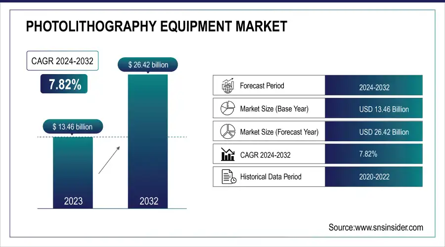
The Photolithography Equipment Market Size was valued at USD 13.46 Billion in 2023 and is expected to reach USD 26.42 Billion by 2032 and grow at a CAGR of 7.82% over the forecast period 2024-2032. The photolithography equipment market is undergoing rapid transformation due to advanced chip-design trends, which are focused on constantly smaller nodes with ever-increasing complexity. The Fab Utilization over the major foundries around the world supports the sustained demand for equipment. EUV equipment penetration is rapidly increasing, and EUV is much more effective at sub-7nm.
Moreover, other technological developments like maskless lithography, better alignment systems, and automation, are also heavily impacting the demand for performance, yield, and manufacturing efficiency within semiconductor manufacturing. The North American region (especially the United States) continued to hold a substantial share of the photolithography equipment market, owing accurately, to its strong semiconductor market and technology. Due to the focus on AI, cloud computing, and data centers in the region, the demand for advanced semiconductor devices has increased the demand for photolithography equipment. Also, there are large semiconductor companies with R&D labs in the U.S. which add to this demand.
To Get more information on Photolithography Equipment Market - Request Free Sample Report
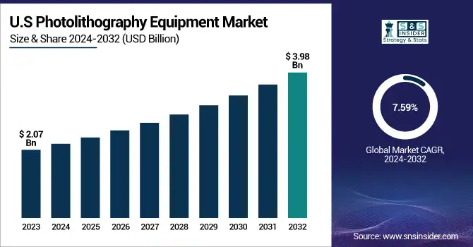
The U.S. Photolithography Equipment Market is estimated to be USD 2.07 Billion in 2023 and expected to reach USD 3.98 Billion is projected to grow at a CAGR of 7.59%. The increasing complexity of integrated circuits, which necessitates advanced patterning techniques, abundant photolithography equipment, and firm collaborations with chipmakers further fueled the growth of the U.S. photolithography equipment market. At the same time, academic collaborations and semiconductor initiatives related to defense are also spurring the development of technology domestically.
Photolithography Equipment Market Dynamics
Key Drivers:
-
Advancing Chip Demand Fuels Photolithography Equipment Growth Across Consumer Automotive and Data Center Applications
The increase in demand for advanced semiconductor nodes is one of the key factors driving the growth of the photolithography equipment market for consumer electronics, automotive, and data centers. The continuous evolution of technologies like AI, 5G, and IoT creates a greater need for high-performance and energy-efficient chips. With this demand, semiconductor manufacturers are moving to shrink down their process nodes (such as 5nm and below), and the newer photolithography technologies on the retailer floor, primarily Extreme Ultraviolet (EUV) systems, need to behave that the turnover of new systems is approx. Moreover, government incentives and subsidies in countries such as the U.S., Europe, and Asia for localizing semiconductor manufacturing are also driving the demand for advanced photolithography tools.
Restrain:
-
Rising Integration Complexity and Precision Demands Pose Challenges for Photolithography Equipment Market Growth
The complexity of integration technology and process finishing is one of the major challenges that is inhibiting the growth of the photolithography equipment market. State-of-the-art photolithography machines, namely EUV, necessitate extremely delicate airer conditions like vacuum chambers, thermal conditions, and ultra-high clean air. Wafers are produced in high precision where even slight changes will end up as defects. Such complexity means that it is reliant on highly skilled labor and expertise, thus bottlenecking production scalability. Even more complex is the continued technical challenge of aligning photomasks with the extreme level of precision needed across more than one layer when fabricating chips, especially at sub-5-nm nodes, where the size of SOI layers is pushed to its theoretical minimum.
Opportunity:
-
Emerging Semiconductor Hubs and Novel Lithography Technologies Unlock New Opportunities for Equipment Vendors Worldwide
One important market opportunity exists in the incorporation of photolithography equipment in up-and-coming semiconductor manufacturing centers. Driven by geopolitical dynamics and the strategy to diversify semiconductor fabrication units, global nations like India and Vietnam have come up with active investments for the same. This paves the way for equipment vendors to step into previously unexplored geographies with customized, economical options in lithography. In addition, advances in both nanoimprint and maskless lithography technologies provide their own set of exciting industry opportunities to enable niche technologies, including MEMS, sensor, and quantum computing for example, so companies can expand their product portfolios and differentiated offerings in next-gen chip manufacturing.
Challenges:
-
Supply Chain Constraints and Geopolitical Risks Challenge Smooth Integration of Photolithography Equipment Components
Another challenge is that most necessary components and materials for photolithography equipment, for example, photoresists, lenses, and light sources are not globally accessible. A limited number of specialist vendors dominate the supply chain for these components, creating a risk of disruptions in the market. As an example, any geopolitical events or restrictions on export can have lots of effects on the manufacturing timeline of the equipment and disrupt the entire process. In addition, with fast-moving technological transitions, it is not easy to collaborate and alignment of all needs from equipment vendors and chip vendors to enable integration of all the parts in a smooth running Semiconductor Fabs at the cutting edge of innovation.
Photolithography Equipment Market Segments Analysis
By Process
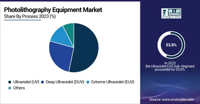
In 2023, the photolithography equipment market was dominated by the Ultraviolet (UV) segment, with a global revenue share of 53.8% share. This is a reflection of the fact that large-node applications include high-volume CMOS image sensors, power devices, and analog ICs, and are typically based on mature manufacturing processes dominated by traditional UV lithography. UV systems are a proven workhorse for high-volume manufacturing, translating to a dependable, cost-efficient option for manufacturers with an eye on the bottom line and legacy chip technologies.
Due to rising demand for advanced node fabrication at and below 7nm and 5nm, the Extreme Ultraviolet (EUV) segment is expected to grow at the fastest rate, with a CAGR between 2024 and 2032. Allows for smaller features and higher resolution, which are critical for the manufacture of high-performance processors used in AI, 5G, and high-end computing. With the expansion of EUV capacity amongst leading foundries such as TSMC, Samsung, and Intel, this segment is set for fast growth.
By Light Source
In 2023, the market share of Excimer Laser was 57.7% and, during the forecast period 2024-2032, it is expected to grow at the highest CAGR. Its predominance can be ascribed to its widespread utilization in DUV and EUV photolithography equipment that plays a critical role in advanced semiconductor fabrication. This is ideal for the patterning needed for high-performance chips, which need the high-energy, short-wavelength light provided by excimer lasers. They have a strong demand for continued technology evolution and their consistent incorporation into more mature as well as cutting-edge lithography tools. Moving forward, with the semiconductor industry's overall gate for scaling smaller nodes and higher transistor densities, the adoption of excimer laser-based systems is expected to ramp up not only to achieve higher market share but to spearhead market growth in the next few years.
By Wave Length
The 70nm – 1nm segment accounted for 51.8% of the total market share in 2023, due to the high penetration of advanced photolithography processes in advanced semiconductor fabrication lines. It is also the main wavelength range used in Extreme Ultraviolet (EUV) lithography, responsible for producing the most advanced chips at 5nm, 3nm, and lower nodes. This segment is further solidified by heavy investments and R&D of leading foundries like TSMC, Samsung, and Intel for EUV systems with changing demands for performance and power, particularly in AI, HPC, and 5G applications.
From 2024 to 2032, the 270nm – 170nm range will rise most rapidly with a CAGR. This range, which aligns with Deep Ultraviolet (DUV) lithography, remains critical for high-volume manufacturing of automotive electronics, IoT, and other mature nodes as well as analog components. The cost-performance balance makes it very appealing for many types of semiconductor applications.
By End Use
Integrated Device Manufacturers (IDMs) with 55.6% market share in 2023 lead the way by encompassing the whole semiconductor production cycle—from design to fabrication under one roof. Such vertical integration enables IDMs to have greater control over manufacturing quality, process optimization, and product innovation. IDMs like Intel, Samsung, and Texas Instruments continue to rack up billable cycles on advanced photolithography tools to meet their in-house product lines across consumer, auto, and industrial with an arsenal of mature and leading-edge chips.
Over the forecast period, 2024 to 2032, foundries are anticipated to achieve the highest CAGR, owing to the increasing adoption of fabless semiconductor trends. With the increasing trend of big chip companies relying on dedicated chip foundries such as TSMC, GlobalFoundries, and UMC, the need for leading-edge photolithography tools will continue to grow. Global foundries are investing in next-generation lithography capabilities in response to expanding demand for AI, 5G, and HPC high-performance chips.
Photolithography Equipment Market Regional Outlook
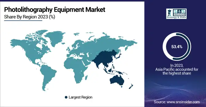
Asia Pacific held the largest market share in 2023, 53.4%, and the region is projected to be the fastest-growing region during the forecast period from 2024 to 2032. * The semiconductor companies and manufacturing tools are concentrated in this region, and hence the intellectual leadership Taiwan, South Korea, China, and Japan are among the largest and most sophisticated semiconductor manufacturers in the world. The mothership of all foundries: the big, bad, giganto, TSMC (Taiwan Semiconductor Manufacturing Company) of China has long led foundry-dom and has made major investments in EUV photolithography for its leading-edge nodes. Another big player, the South Korean company Samsung Electronics, is aggressively building out its semiconductor capacity. As most of its national strategy for self-reliance, China is aggressively ramping up its local semiconductor manufacturing led by companies such as SMIC (Semiconductor Manufacturing International Corporation). Moreover, Japan is essential for providing photolithography materials and components, such as photoresists and optics. These real-world instances drive home the point that Asia Pacific continues to be the leading and fastest-growing region in the global photolithography equipment market.
Get Customized Report as per Your Business Requirement - Enquiry Now
Key Players Listed in Photolithography Equipment Market are:
-
ASML (TWINSCAN NXE:3600D)
-
Nikon Corporation (NSR-S636E)
-
Canon Inc. (FPA-5550iZ2)
-
Veeco Instruments Inc. (NEXUS Lithography)
-
Ultratech (acquired by Veeco) (Sapphire 100)
-
SÜSS MicroTec (MA300 Gen3)
-
EV Group (EVG) (EVG620 NT)
-
JEOL Ltd. (JBX-8100FS)
-
Rudolph Technologies (Onto Innovation) (JetStep S)
-
Tamarack Scientific Co., Inc. (MLA-150 Maskless Lithography)
-
SMEE (Shanghai Micro Electronics Equipment) (SSA/600 series)
-
Orbotech (acquired by KLA) (Paragon Xpress)
-
NuFlare Technology (a subsidiary of Toshiba) (EBM-9000)
-
SCREEN Semiconductor Solutions (SK-P1500)
-
Neutronix Quintel (NXQ4006)
Photolithography Equipment Market Trends
-
In October 2024, Nikon announced the development of a digital lithography system with 1.0 µm (L/S) resolution, set for release in FY2026. The system features a maskless design using a spatial light modulator, targeting advanced semiconductor packaging.
-
In September 2025, Canon delivered its FPA-1200NZ2C nanoimprint lithography system to the Texas Institute for Electronics for advanced semiconductor manufacturing.
| Report Attributes | Details |
|---|---|
| Market Size in 2023 | USD 13.46 Billion |
| Market Size by 2032 | USD 26.42 Billion |
| CAGR | CAGR of 7.82% From 2024 to 2032 |
| Base Year | 2023 |
| Forecast Period | 2024-2032 |
| Historical Data | 2020-2022 |
| Report Scope & Coverage | Market Size, Segments Analysis, Competitive Landscape, Regional Analysis, DROC & SWOT Analysis, Forecast Outlook |
| Key Segments | • By Process (Ultraviolet UV, Deep Ultraviolet (DUV), Extreme Ultraviolet (EUV), Others) • By Light Source (Mercury Lamp, Fluorine Laser, Excimer Laser, Others) • By Wave Length (370nm -270nm, 270nm - 170nm, 70nm - 1nm) • By End Use (Integrated Device Manufacturer (IDMs), Foundries) |
| Regional Analysis/Coverage | North America (US, Canada, Mexico), Europe (Eastern Europe [Poland, Romania, Hungary, Turkey, Rest of Eastern Europe] Western Europe] Germany, France, UK, Italy, Spain, Netherlands, Switzerland, Austria, Rest of Western Europe]), Asia Pacific (China, India, Japan, South Korea, Vietnam, Singapore, Australia, Rest of Asia Pacific), Middle East & Africa (Middle East [UAE, Egypt, Saudi Arabia, Qatar, Rest of Middle East], Africa [Nigeria, South Africa, Rest of Africa], Latin America (Brazil, Argentina, Colombia, Rest of Latin America) |
| Company Profiles | ASML, Nikon Corporation, Canon Inc., Veeco Instruments Inc., Ultratech, SÜSS MicroTec, EV Group, JEOL Ltd., Rudolph Technologies, Tamarack Scientific Co., Inc., SMEE, Orbotech, NuFlare Technology, SCREEN Semiconductor Solutions, Neutronix Quintel. |
Frequently Asked Questions
Ans: In 2023, the Asia Pacific region led the Photolithography Equipment market, capturing approximately 53.45% of the total market share.
Ans: The Ultraviolet UV segment dominated the Photolithography Equipment market in 2023.
Ans: Rising demand for advanced semiconductor nodes, increased adoption of EUV technology, and growth in AI, 5G, and automotive electronics are key drivers of the photolithography equipment market.
Ans: The Photolithography Equipment Market size was USD 13.46 billion in 2023 and is expected to Reach USD 26.42 billion by 2032.
Ans: The Photolithography Equipment Market is expected to grow at a CAGR of 7.82%.
Get in Touch
