
Photoresist Market Report Scope & Overview:
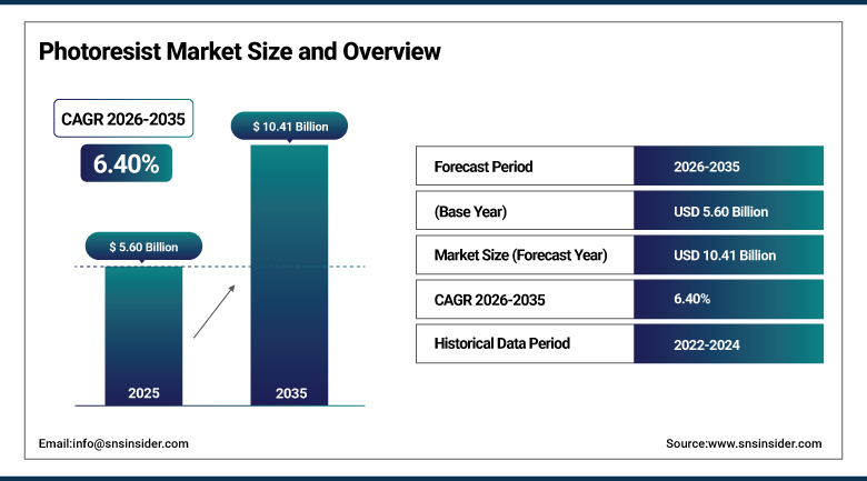
The Photoresist Market was valued at USD 5.60 Billion in 2025 and is expected to reach USD 10.41 Billion by 2035, growing at a CAGR of 6.40% from 2026-2035.
The Photoresist Market covers the light-sensitive polymer materials, and the ancillary coatings, developers and removers, used to transfer circuit patterns onto silicon wafers, packaging substrates, printed circuit boards and display panels during photolithography. Resists are formulated for specific exposure wavelengths, from g-line and i-line to KrF, ArF, ArF immersion and extreme ultraviolet, and each new chip generation demands tighter purity, resolution and defect control. Demand follows semiconductor capacity, advanced packaging and display production, and supply is concentrated among a handful of Japanese, American, European and Korean chemical groups. Customers qualify resists for years, which makes switching rare and favors suppliers that co-develop products alongside leading chipmakers.
⮞In early April 2026, JSR formed a joint venture with Taiwanese partners Wah Lee Industrial and LCY Chemical to build its first photoresist plant in Taiwan, in Yunlin County, with operations expected as early as 2028. The plant is intended to co-develop advanced resists, including metal oxide resists for EUV lithography, with TSMC, and JSR later opened a planarization research center in Hukou, Hsinchu County, with TSMC and Applied Materials. JSR's metal oxide resist plant in Cheongju, South Korea, is also expected to start mass production in 2026.
To Get more information Photoresist Market - Request Free Sample Report
Photoresist Market Trends
-
Shift toward EUV and metal oxide resists for sub-3 nm chip nodes
-
Local production of resists near leading foundries in Taiwan and South Korea
-
PFAS-free resist formulations responding to environmental pressure
-
Growth of resists for advanced packaging and chiplet interconnects
-
Co-development agreements between resist makers, foundries and tool suppliers
-
Rising purity and defect control requirements in resists and ancillaries
U.S. Photoresist Market Outlook
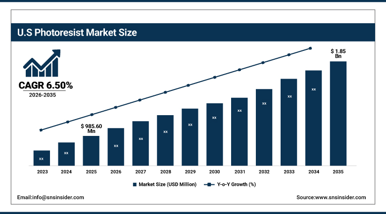
The U.S. Photoresist Market was valued at USD 985.60 Million in 2025 and is expected to reach USD 1.85 Billion by 2035, growing at a CAGR of 6.50% from 2026-2035.
The U.S. Photoresist Market is the largest national market in North America, led by demand from fabs in Arizona, Texas, Oregon, New York and Idaho, along with advanced packaging, MEMS and research users. CHIPS Act funding is supporting new fabs and encouraging materials suppliers to localize production, although most advanced resists are still imported from Japan, Korea and Europe. American suppliers such as DuPont and Fujifilm Electronic Materials' U.S. sites serve specialty and legacy nodes and advanced packaging. Export controls and tariffs on chemicals add uncertainty, and customers value supply security alongside performance.
⮞At SEMICON West 2025, held October 7-9 in Phoenix, Fujifilm showcased EUV, ArF, KrF, i-line and legacy photoresists, including new PFAS-free resists, along with CMP slurries, process chemicals, polyimide packaging materials and low-K dielectric precursors. The company noted it runs 20 manufacturing sites worldwide, including six U.S. facilities and research labs in Arizona, California, Colorado, Rhode Island and Texas. The one-stop approach reflects how U.S. fabs want fewer qualified suppliers with local support.
Photoresist Market Segment Analysis
-
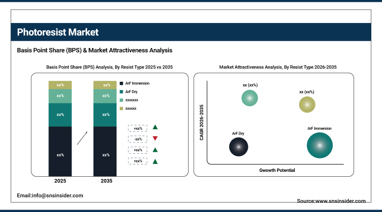
By Resist Type, the ArF Immersion segment dominated the Photoresist Market with approximately 35.00% share in 2025, while the EUV segment is the fastest growing with a CAGR of approximately 12.40%.
-
By Tone, the Positive-Tone segment dominated the Photoresist Market with approximately 73.00% share in 2025, while the Negative-Tone segment is the fastest growing with a CAGR of approximately 10.90%.
-
By Application, the Semiconductors and ICs segment dominated the Photoresist Market with approximately 50.00% share in 2025, while the Advanced Packaging segment is the fastest growing with a CAGR of approximately 11.00%.
-
By End-Use Industry, the Electronics and Electricals segment dominated the Photoresist Market with approximately 62.00% share in 2025, while the Automotive and Mobility segment is the fastest growing with a CAGR of approximately 9.90%.
-
By Ancillary Type, the Anti-Reflective Coatings segment dominated the Photoresist Market with approximately 44.82% share in 2025, while the Removers segment is the fastest growing with a CAGR of approximately 5.92%.
By Resist Type, ArF Immersion Dominates the Photoresist Market and EUV Grows Fastest
ArF immersion resists lead because they pattern the most critical layers in leading-edge logic and memory chips at 193 nm, using water between the lens and the wafer to improve resolution. Foundries run multiple exposures with ArF immersion for nodes below 10 nm, so consumption per wafer is high. Suppliers such as TOK, JSR, Shin-Etsu, Sumitomo and Fujifilm hold deep qualifications, and the installed base of immersion scanners keeps this resist type at roughly 35% of revenue.
EUV resists are growing fastest because every new advanced node adds EUV layers, and high-NA EUV systems require resists with higher sensitivity and lower roughness. Metal oxide resists, such as those from JSR's Inpria unit, are emerging as an alternative to chemically amplified resists. JSR's planned Korean plant and its Taiwan joint venture, along with TOK's investment in Korea, show suppliers building capacity. From a small base, EUV resist volumes rise quickly with each fab expansion.
By Tone, Positive-Tone Dominates the Photoresist Market and Negative-Tone Grows Fastest
Positive-tone resists lead because exposed areas become soluble in developer, which gives high resolution and a straightforward process for most semiconductor layers. They have been the standard for decades across g-line, i-line, KrF and ArF generations, and process engineers know how to tune them. Their wide use in leading-edge and mature fabs gives positive-tone products almost three quarters of revenue.
Negative-tone resists are growing fastest because certain applications, such as thick films for advanced packaging, MEMS, micro-bumps and some negative-tone development processes at advanced nodes, perform better with exposed areas that remain. Packaging houses use thick negative resists for redistribution layers and copper pillars, and chipmakers use negative-tone development for contact and trench patterns. Growth in chiplet and high-bandwidth memory packaging supports the segment.
By Application, Semiconductors and ICs Dominates the Photoresist Market and Advanced Packaging Grows Fastest
Semiconductors and ICs lead because wafer fabrication uses the largest volume and highest-value resists, with dozens of lithography steps per chip. Logic, memory, analog and power devices all rely on photoresist, and the build-out of fabs in Taiwan, South Korea, Japan, the United States and China sustains demand. Artificial intelligence processors and high-bandwidth memory require leading-edge layers, which keeps resist spending tied to wafer starts.
Advanced packaging is growing fastest because 2.5D and 3D integration, chiplets and fan-out designs need fine-pitch redistribution layers, bumps and through-silicon vias, all patterned with specialized resists and dielectrics. Memory and AI accelerator makers are expanding packaging capacity quickly, and TOK is investing in a Korean plant to serve packaging resist demand from Samsung and SK hynix. Fujifilm and others are offering polyimide and resist portfolios aimed at this segment.
By End-Use Industry, Electronics and Electricals Dominates the Photoresist Market and Automotive and Mobility Grows Fastest
Electronics and electricals lead because consumer devices, computers, servers, networking gear and industrial electronics account for the bulk of chip, PCB and display output. Smartphones, PCs and data center hardware drive wafer demand, and electronics makers also use resists in circuit boards and sensors. This broad base gives the end-use roughly 62% of revenue, although cycles in consumer demand can move volumes.
Automotive and mobility is growing fastest as vehicles add power semiconductors, sensors, microcontrollers and driver assistance chips. Electric vehicles use silicon carbide and other power devices that rely on mature-node lithography, and autonomous features use advanced processors. Automakers also require long-term supply agreements and high reliability, which supports qualified suppliers. From a smaller base, automotive resist consumption grows faster than consumer electronics.
By Ancillary Type, Anti-Reflective Coatings Dominates the Photoresist Market and Removers Grows Fastest
Anti-reflective coatings lead the ancillary products because they are applied under or over the resist to control reflections that blur patterns, and they are needed in almost all advanced lithography steps. Grand View Research puts their share of photoresist ancillaries at about 44.82% in 2024. Spin-on bottom coatings and developable layers are qualified together with the resist, so ARC purchases rise with each lithography layer.
Removers are growing fastest because every patterned layer must be stripped cleanly, and more complex stacks, high-aspect-ratio structures and new metal and metal oxide materials need tailored chemistries. Environmental rules push suppliers toward less hazardous solvents, and the increase in lithography layers per chip raises removal volumes. Grand View Research projects a CAGR near 5.92% for removers, the fastest among ancillary types.
Regional Analysis
|
Region |
Major Country |
Share within Region, 2025 (%) |
|---|---|---|
|
Asia Pacific |
Taiwan |
31.00 |
|
North America |
United States |
88.00 |
|
Europe |
Germany |
34.00 |
|
Middle East & Africa |
Israel |
45.00 |
|
Latin America |
Brazil |
41.00 |
Asia Pacific Photoresist Market Insights
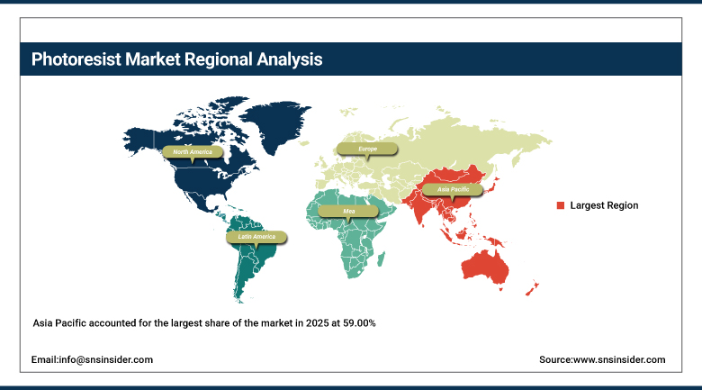
Asia Pacific accounted for the largest share of the market in 2025 at 59.00% and is also the fastest-growing region, advancing at a CAGR of 6.90% through 2035. Taiwan, South Korea, Japan and China lead through foundry, memory and packaging capacity, and Japan hosts the leading suppliers TOK, JSR, Shin-Etsu and Sumitomo.
⮞Resist makers are expanding near customers. JSR's Yunlin County joint venture is expected online as early as 2028, TOK announced a JPY 20 billion Korean photoresist plant for Samsung and SK hynix operating from 2030, and Shin-Etsu is building a JPY 83 billion facility in Gunma. China is building local resist capacity from i-line to ArF, but EUV remains dependent on imports.
Get Customized Report as per Your Business Requirement - Enquiry Now
North America Photoresist Market Insights
North America held 20.00% of the market in 2025 and is growing at a CAGR of 6.60% through 2035. The United States holds most regional value through fabs in Arizona, Texas, Oregon, New York and Idaho, as well as packaging and research users, and Canada and Mexico add smaller volumes.
CHIPS Act support is bringing new fabs, and suppliers such as Fujifilm and DuPont maintain regional production and technical support. Advanced EUV resists are largely imported, so supply-chain security is a purchasing criterion. Tariff and export control uncertainty is a risk, but the fab pipeline supports steady growth.
Europe Photoresist Market Insights
Europe held 15.00% of the market in 2025 and is growing at a CAGR of 5.40% through 2035. Germany, France, Italy, the Netherlands, Ireland and Belgium lead through automotive and power semiconductor fabs, research centers such as imec, and the EUV scanner supply chain around ASML.
Merck KGaA, BASF, Allresist and micro resist technology supply specialty and research resists, and the European Chips Act aims to raise regional capacity. Strong automotive and industrial chip demand supports mature-node lithography, while limited leading-edge fab capacity restrains growth in advanced resists.
MEA & Latin America Photoresist Market Insights
The Middle East and Africa held 3.20% of the market and is growing at a CAGR of 5.80%. Israel leads through large fabs and design centers, with the United Arab Emirates and Saudi Arabia exploring semiconductor investment. Nearly all resists are imported from Asia, the United States and Europe.
Latin America held 2.80% of the market and is growing at a CAGR of 5.50%. Brazil and Mexico lead through electronics assembly, packaging and some device manufacturing, with Costa Rica adding assembly and test. Small fab capacity limits demand, but electronics manufacturing and nearshoring support steady volumes.
Market Dynamics
Growth Drivers: Leading-Edge Fab Expansion, AI Chip Demand and Advanced Packaging
Leading-edge fab expansion is the primary driver. Foundries and memory makers are building capacity at 3 nm, 2 nm and beyond, and each node adds lithography layers, many with EUV and multiple ArF immersion exposures. Resist consumption rises with wafer starts and layer counts, and long-term supply agreements with chipmakers give suppliers visibility to invest in new plants.
AI chip demand and advanced packaging add momentum. Accelerators and high-bandwidth memory require leading-edge wafers and complex packaging with fine-pitch interconnects, both of which use specialized resists. Suppliers are launching new products and building capacity near customers, as shown by JSR in Taiwan and Korea and TOK in Korea, to shorten supply chains and improve co-development.
Restraints: Supplier Concentration, Qualification Cycles and Raw Material Constraints
Supplier concentration is a significant restraint. A few Japanese companies supply most advanced resists, and geopolitical tension or natural disasters can disrupt supply, as seen in past export disputes. Chipmakers must qualify new suppliers over years, which limits competition and slows market entry for new producers.
Qualification cycles and raw material constraints add pressure. Photoresists depend on high-purity polymers, photoacid generators and solvents from a limited set of sources, and metal oxide resists need specialty precursors. Regulatory pressure on PFAS compounds forces reformulation, which adds cost and testing time, and plant construction takes years before capacity arrives.
Opportunities: Metal Oxide Resists, PFAS-Free Formulations and Local Supply
Metal oxide resists offer a major opportunity as EUV patterning moves to finer pitches and high-NA tools. Their high absorption and etch resistance can improve resolution and reduce defects, and JSR's Cheongju plant and Taiwan joint venture are aimed at this technology. Early partnerships with TSMC, Samsung and others give suppliers an advantage in qualifying new products.
PFAS-free formulations and local supply provide further opportunities. Fujifilm and others are introducing PFAS-free resists to meet customer and regulatory demand, and chipmakers want suppliers located near fabs for security and responsiveness. Companies that can offer resists, ancillaries and process chemicals together, close to customers, can win larger shares of spending.
Recent Developments:
-
2026: JSR opened a planarization research center in Hukou, Hsinchu County, with TSMC and Applied Materials, and its metal oxide resist plant in Cheongju, South Korea, is expected to start mass production in 2026.
-
2026: reports noted Shin-Etsu Chemical is building a JPY 83 billion facility in Isesaki, Gunma Prefecture, to expand lithography materials capacity.
-
2025: Tokyo Ohka Kogyo announced a JPY 20 billion photoresist plant in South Korea to serve Samsung Electronics and SK hynix, expanding its Korean capacity three to four times, with operations scheduled for 2030.
Photoresist Market Key Players are
-
Tokyo Ohka Kogyo Co., Ltd.
-
JSR Corporation
-
Shin-Etsu Chemical Co., Ltd.
-
FUJIFILM Holdings Corporation
-
Sumitomo Chemical Co., Ltd.
-
DuPont de Nemours, Inc.
-
Merck KGaA (EMD Electronics)
-
Dongjin Semichem Co., Ltd.
-
LG Chem Ltd.
-
Kolon Industries, Inc.
-
Asahi Kasei Corporation
-
Eternal Materials Co., Ltd.
-
Everlight Chemical Industrial Corporation
-
Brewer Science, Inc.
-
Inpria Corporation
-
Allresist GmbH
-
MicroChemicals GmbH
-
micro resist technology GmbH
-
Jiangsu Nata Opto-electronic Material Co., Ltd.
-
Kempur Microelectronics, Inc.
-
BASF SE
Photoresist Market Report Scope:
| Report Attributes | Details |
|---|---|
| Market Size in 2025 | USD 5.60 Billion |
| Market Size by 2035 | USD 10.41 Billion |
| CAGR | CAGR of 6.40% From 2026 to 2035 |
| Base Year | 2025 |
| Forecast Period | 2026-2035 |
| Historical Data | 2022-2024 |
| Report Scope & Coverage | Market Size, Segments Analysis, Competitive Landscape, Regional Analysis, DROC & SWOT Analysis, Forecast Outlook |
| Key Segments | • By Resist Type (ArF Immersion, ArF Dry, KrF, EUV, I-Line and G-Line, Others) • By Tone (Positive-Tone, Negative-Tone) • By Application (Semiconductors and ICs, Advanced Packaging, PCBs, LCDs and Displays, Others) • By End-Use Industry (Electronics and Electricals, Automotive and Mobility, Telecommunications, Healthcare, Others) • By Ancillary Type (Anti-Reflective Coatings, Developers, Removers, Others) |
| Regional Analysis/Coverage | North America (US, Canada), Europe (Germany, UK, France, Italy, Spain, Russia, Poland, Rest of Europe), Asia Pacific (China, India, Japan, South Korea, Australia, ASEAN Countries, Rest of Asia Pacific), Middle East & Africa (UAE, Saudi Arabia, Qatar, South Africa, Rest of Middle East & Africa), Latin America (Brazil, Argentina, Mexico, Colombia, Rest of Latin America). |
| Company Profiles | Tokyo Ohka Kogyo Co., Ltd., JSR Corporation, Shin-Etsu Chemical Co., Ltd., FUJIFILM Holdings Corporation, Sumitomo Chemical Co., Ltd., DuPont de Nemours, Inc., Merck KGaA (EMD Electronics), Dongjin Semichem Co., Ltd., LG Chem Ltd., Kolon Industries, Inc., Asahi Kasei Corporation, Eternal Materials Co., Ltd., Everlight Chemical Industrial Corporation, Brewer Science, Inc., Inpria Corporation, Allresist GmbH, MicroChemicals GmbH, Jiangsu Nata Opto-electronic Material Co., Ltd., Kempur Microelectronics, Inc., BASF SE |

Frequently Asked Questions
Key players include Tokyo Ohka Kogyo, JSR, Shin-Etsu Chemical, FUJIFILM, Sumitomo Chemical, DuPont, Merck KGaA, Dongjin Semichem, LG Chem, Kolon Industries, Asahi Kasei, Eternal Materials, Brewer Science, Inpria and Allresist.
Key opportunities include metal oxide EUV resists, PFAS-free formulations, resists for advanced packaging and local production close to leading foundries.
The major growth factor is leading-edge fab expansion, because each new node adds lithography layers, with EUV and ArF immersion exposures raising resist consumption per wafer.
By Resist Type, the ArF Immersion segment dominated the market with approximately 35.00% share in 2025, owing to its use in the most critical layers of advanced logic and memory chips.
Asia Pacific dominated the market with a share of 59.00% in 2025, supported by foundry, memory and packaging capacity in Taiwan, South Korea, Japan and China and by leading Japanese suppliers.
