
Semiconductor Chemical Vapor Deposition Equipment Market Report Scope & Overview:
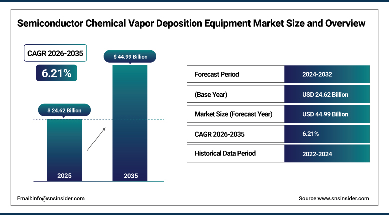
The Semiconductor Chemical Vapor Deposition Equipment Market was valued at USD 24.62 Billion in 2025 and is expected to reach USD 44.99 Billion by 2035, growing at a CAGR of 6.21% from 2026 to 2035.
The Semiconductor Chemical Vapor Deposition Equipment Market is growing due to increasing demand for semiconductor chips, increased investment in semiconductor manufacturing plants, and developments in the AI, 5G, and high-performance computing industry sectors. Adoption of advanced process node, 3D NAND, DRAM, and logic semiconductor manufacturing technology is expected to lead to a higher demand for deposition equipment. Moreover, technological advancements in chemical vapor deposition, plasma-enhanced chemical vapor deposition, and atomic layer deposition, along with developments in compound semiconductors and capacity increase in wafers, are some other factors boosting the market growth.
December 2024, ULVAC has released ENTRON-EXX, a generalized multi-chamber deposition system for semiconductor production, to enhance productivity and shorten development time by utilizing advanced data acquisition and expandability.
To Get more information Semiconductor Chemical Vapor Deposition Equipment Market - Request Free Sample Report
Semiconductor Chemical Vapor Deposition Equipment Market Trends:
-
Rising demand for advanced semiconductor chips driving adoption of chemical vapor deposition (CVD) equipment in wafer fabrication processes
-
Growing expansion of semiconductor manufacturing facilities and foundries increasing investments in high-precision deposition technologies
-
Increasing production of 3D NAND, advanced logic chips, and power semiconductors boosting the need for uniform thin-film deposition solutions
-
Expanding adoption of advanced materials such as silicon carbide (SiC), gallium nitride (GaN), and compound semiconductors supporting CVD equipment demand
-
Continuous advancements in atomic layer deposition (ALD), plasma-enhanced CVD, and process automation improving film quality, efficiency, and semiconductor manufacturing yields
U.S. Semiconductor Chemical Vapor Deposition Equipment Market Outlook:
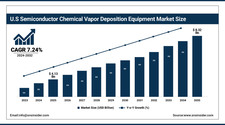
The U.S. Semiconductor Chemical Vapor Deposition Equipment Market was valued at approximately USD 4.13 Billion in 2025 and is expected to reach approximately USD 8.32 Billion by 2035, growing at a CAGR of approximately 7.24%.
The United States is the world's most significant semiconductor CVD equipment development and manufacturing centre within the North American region, anchored by Applied Materials and Lam Research whose combined CVD and related deposition equipment revenues represent the largest national concentration of semiconductor process equipment capability globally.
The CHIPS and Science Act's USD 52.7 billion semiconductor investment programme, which includes USD 39 billion in manufacturing incentives and USD 13.2 billion in research and development funding, is stimulating the most concentrated domestic semiconductor fab construction investment in decades at TSMC's Arizona facilities, Intel's Ohio and Arizona expansion, Samsung's Texas fab, and Micron's Idaho and New York investments whose aggregate CVD equipment procurement through 2030 represents many billions of dollars of domestic market demand.
AIXTRON SE launched its MOCVD G5+ C equipment for compound semiconductor epitaxial deposition in 2025, targeting GaN-on-silicon epitaxy for power electronics applications including 5G base station power amplifiers, electric vehicle charging converters, and solar inverter power stages whose efficiency performance advantages over silicon MOSFET alternatives justify the higher initial substrate and wafer cost of GaN-on-Si epitaxial material.
Semiconductor Chemical Vapor Deposition Equipment Market Segment Analysis:
-
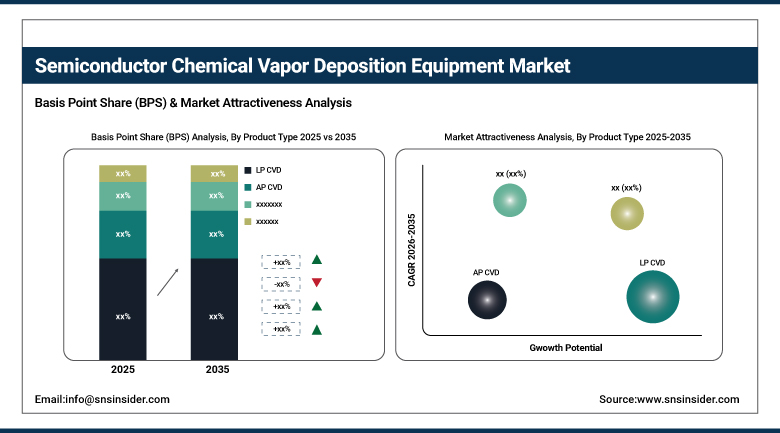
By Product Type, Low-pressure Chemical Vapor Deposition (LP CVD) segment dominated the Semiconductor Chemical Vapor Deposition Equipment Market in 2025 with 38% share; Metal-organic Chemical Vapor Phase Deposition (MO CVD) segment is the fastest growing segment.
-
By Application, Memory Chips segment dominated the market in 2025 with 35% share; Logic Chips segment is the fastest growing segment.
By Product Type, Low-pressure Chemical Vapor Deposition (LP CVD) segment dominates the Market, Metal-organic Chemical Vapor Phase Deposition (MO CVD) segment expected to grow fastest
The Low-pressure Chemical Vapor Deposition (LP CVD) segment dominated the Semiconductor Chemical Vapor Deposition Equipment Market in 2025 due to its extensive use in the fabrication of semiconductors through which high-quality thin films can be produced with high uniformity and accuracy. The use of LP CVD is extensive in memory devices, logic elements, and semiconductor devices. Its capabilities for mass production, better process control, and high deposition performance have resulted in its increasing adoption. The demand for advanced chips and semiconductor miniaturization has further reinforced the segment's market leadership.
The Metal-organic Chemical Vapor Phase Deposition (MO CVD) segment is the fastest growing due to the increasing demand for compound semiconductors and advanced electronic components. MO CVD technology allows for accurate deposition of materials for usage in electronic devices like LEDs, power electronics, optical devices, and high frequency parts. The rising adoption of materials such as gallium nitride and other wide band gap semiconductor materials is driving the demand for MO CVD. Investments in next generation semiconductors, electric vehicles, and high-performance computing are aiding segment growth.
By Application, Memory Chips segment dominates the Semiconductor Chemical Vapor Deposition Equipment Market, Logic Chips segment expected to grow fastest
The Memory Chips segment dominated the Semiconductor Chemical Vapor Deposition Equipment Market in 2025 owing to the significant utilization of CVD equipment in the production of advanced memory such as DRAM and NAND flash. The use of CVD equipment is essential in the deposition of quality thin films needed in advanced memory technology. High demand for memory in storage, cloud computing, artificial intelligence, and consumer electronics has led to an increase in the production of semiconductors. Constant development in memory production has also contributed to this segment's dominance.
The Logic Chips segment is the fastest growing in the Semiconductor Chemical Vapor Deposition Equipment Market owing to the increased need for advanced processors in AI, high-performance computing, automotive electronics, and connected devices. Semiconductor producers are making efforts towards the advancement in production of semiconductors using sophisticated deposition technology that increases performance and makes the chips small. Demand is fueled by the rising edge computing, autonomous vehicles, and future electronic systems. Constant development in semiconductor architecture has further boosted the segment's growth.
Regional Analysis:
|
Region |
Major Country |
Share within Region, 2025 (%) |
|---|---|---|
|
North America |
United States |
84.73% |
|
Europe |
Germany |
27.84% |
|
Asia Pacific |
Taiwan |
28.47% |
|
Middle East & Africa |
UAE |
22.84% |
|
Latin America |
Brazil |
43.84% |
North America Semiconductor CVD Equipment Market Insights
North America held approximately 20.00% of global Semiconductor CVD Equipment revenues in 2025, anchored by the domestic headquarters of Applied Materials and Lam Research whose combined semiconductor process equipment revenues make North America the world's dominant CVD equipment design and manufacturing centre even as the majority of equipment units are deployed in Asian manufacturing facilities. The CHIPS Act's domestic fab construction investment is creating incremental North American CVD equipment installation that progressively increases the region's share of global CVD equipment operating base beyond its current 20 percent revenue share.
Europe Semiconductor CVD Equipment Market Insights
Europe held approximately 12.00% of global Semiconductor CVD Equipment revenues in 2025. Germany accounts for approximately 27.84% of European revenues through AIXTRON SE's MOCVD equipment manufacturing, Infineon Technologies' SiC power semiconductor CVD epitaxial growth equipment procurement, and the European semiconductor equipment ecosystem that includes tool manufacturers serving both domestic and global semiconductor manufacturing customers. The EU Chips Act's 43 billion Euro semiconductor investment programme is stimulating European fab construction investment that will incrementally grow European CVD equipment installation. ASM International's Netherlands headquarters contributes European CVD and ALD equipment revenue.
Asia Pacific Semiconductor CVD Equipment Market Insights
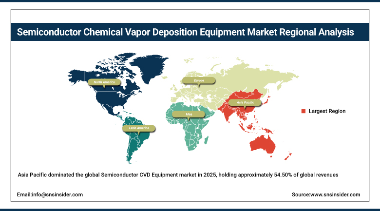
Asia Pacific dominated the global Semiconductor CVD Equipment market in 2025, holding approximately 54.50% of global revenues through the concentration of the world's largest semiconductor fabrication facilities at TSMC in Taiwan, Samsung and SK Hynix in South Korea, and SMIC, YMTC, and other domestic Chinese chip manufacturers. Taiwan accounts for approximately 28.47% of Asia Pacific revenues through TSMC's dominant position as the world's largest contract chipmaker whose annual capital expenditure on process equipment represents the single largest semiconductor equipment procurement programme globally. South Korea contributes through Samsung's and SK Hynix's memory and foundry CVD procurement. China is growing rapidly through domestic semiconductor investment as the National Integrated Circuit Industry Investment Fund sustains fab capacity expansion.
Get Customized Report as per Your Business Requirement - Enquiry Now
MEA & Latin America Semiconductor CVD Equipment Market Insights
Middle East and Latin America represent smaller but developing Semiconductor CVD Equipment markets where government-funded semiconductor manufacturing investment and research facility expansion are creating initial CVD equipment procurement. The UAE leads MEA revenues at approximately 22.84% of the regional total through its advanced manufacturing investment in semiconductor-adjacent industries and research facility development. Saudi Arabia's NEOM and Vision 2030 digital technology investment includes semiconductor research capability development. Brazil leads Latin American revenues at approximately 43.84% of the regional total through its domestic IC design and packaging sector and research institution CVD equipment procurement.
Market Dynamics:
Growth Drivers: Advanced semiconductor scaling and 3D NAND expansion are driving next-generation CVD equipment demand
The semiconductor industry's continuous technology node progression creates a recurring CVD equipment upgrade cycle whose commercial scale is proportional to the aggregate capital expenditure of the world's leading semiconductor manufacturers. Each node transition requires CVD equipment whose deposition precision, uniformity, selectivity, and throughput exceed the capability of the prior generation's tools, creating a technology refresh requirement that sustains CVD equipment procurement independent of capacity addition.
The gate-all-around transistor architecture's adoption at 2 nanometre logic nodes requires CVD and ALD processes for nanosheet semiconductor material deposition, spacer formation, and gate dielectric growth whose precision at sub-10 angstrom dimensions represents the current frontier of commercial deposition equipment capability. 3D NAND memory manufacturers escalating layer counts from 128 to 232 to 300 and beyond require HDPCVD systems capable of achieving conformal oxide-nitride layer deposition within trenches whose 50:1 aspect ratio creates deposition uniformity challenges that push the limits of current plasma enhanced CVD process physics.
Restraints: High equipment costs and geopolitical export restrictions constrain semiconductor CVD market development
Advanced CVD equipment systems for leading-edge logic and memory fabrication carry unit prices ranging from USD 5 million to USD 50 million per chamber cluster system depending on process complexity, wafer handling integration, and process capability specification, creating capital intensity that constrains the speed of capacity addition at existing and new fabrication facilities.
The U.S. government's export control regulations governing the supply of advanced semiconductor manufacturing equipment to certain countries, including the Foreign Direct Product Rule's application to entities and countries subject to advanced technology export restrictions, creates market segmentation where the leading-edge CVD equipment market is effectively limited to qualified end-users in allied country semiconductor manufacturing programmes.
Opportunities: SiC epitaxial and GaN MOCVD equipment offer high-growth compound semiconductor opportunities.
Silicon carbide MOSFET adoption in EV power electronics is creating sustained demand growth for SiC CVD epitaxial growth reactors whose hot-wall reactor design deposits SiC epilayers of precisely controlled doping profile, defect density, and thickness uniformity on SiC substrates at temperatures of 1,550 to 1,650 degrees Celsius.
The EV market's projected growth toward 40 million annual vehicle sales by 2030 creates aggregate SiC MOSFET demand whose wafer equivalent area growth is proportional to power electronics content per vehicle, sustaining investment in SiC CVD epitaxial capacity at Wolfspeed, Onsemi, Rohm, and Infineon's SiC manufacturing facilities. GaN-on-Si MOCVD equipment growth is sustained by the expanding 5G power amplifier market for base stations and the EV onboard charger market for GaN power transistors whose higher switching frequency enables smaller, lighter charger designs whose consumer market value justifies GaN's initial cost premium over silicon alternatives.
Recent Developments:
-
2025: Applied Materials reported continued strong CVD equipment demand from TSMC, Samsung, and Intel Foundry at leading logic nodes, with the Centura integrated process platform capturing leading-edge gate-all-around transistor CVD and ALD deposition share through its vacuum-integrated multi-step process architecture.
-
2025: AIXTRON SE launched the MOCVD G5+ C for GaN-on-silicon epitaxy targeting EV power electronics and 5G base station power amplifier applications, featuring planetary wafer rotation and optimised gas injection for improved GaN uniformity across 200 mm substrates supporting cost-effective power device manufacturing.
-
2025: Lam Research reported strong demand for its PECVD and HDPCVD systems from 3D NAND memory manufacturers whose 200 to 400+ layer architecture programmes require high-aspect-ratio dielectric deposition capability continuously advancing the technical limits of commercial PECVD process physics.
Semiconductor CVD Equipment Market Key Players are:
-
Applied Materials, Inc.
-
Lam Research Corporation
-
Tokyo Electron Limited
-
ASM International N.V.
-
Kokusai Electric Corporation
-
Hitachi High-Technologies Corporation
-
SCREEN Semiconductor Solutions Co., Ltd.
-
Veeco Instruments Inc.
-
Aixtron SE
-
CVD Equipment Corporation
-
Kurt J. Lesker Company
-
Oxford Instruments plc
-
Plasma-Therm LLC
-
SPTS Technologies (KLA Corporation)
-
Ulvac, Inc.
-
Samco Inc.
-
Lamda Systems Inc.
-
Jusung Engineering Co., Ltd.
-
Wonik IPS Co., Ltd.
-
Eugene Technology Co., Ltd.
Semiconductor Chemical Vapor Deposition Equipment Market Report Scope:
| Report Attributes | Details |
|---|---|
| Market Size in 2025 | USD 24.62 Billion |
| Market Size by 2035 | USD 44.99 Billion |
| CAGR | CAGR of 6.21% From 2026 to 2035 |
| Base Year | 2025 |
| Forecast Period | 2026-2035 |
| Historical Data | 2022-2024 |
| Report Scope & Coverage | Market Size, Segments Analysis, Competitive Landscape, Regional Analysis, DROC & SWOT Analysis, Forecast Outlook |
| Key Segments | • By Product Type (Atmospheric-Pressure Chemical Vapor Deposition , Density-Plasma Chemical Vapor Deposition , Low-pressure Chemical Vapor Deposition , Metal-organic Chemical Vapor Phase Deposition) • By Application (Logic Chips, Memory Chips, Analog Chips, Optoelectronics, Discretes, Sensors) |
| Regional Analysis/Coverage | North America (US, Canada), Europe (Germany, UK, France, Italy, Spain, Russia, Poland, Rest of Europe), Asia Pacific (China, India, Japan, South Korea, Australia, ASEAN Countries, Rest of Asia Pacific), Middle East & Africa (UAE, Saudi Arabia, Qatar, South Africa, Rest of Middle East & Africa), Latin America (Brazil, Argentina, Mexico, Colombia, Rest of Latin America). |
| Company Profiles | Applied Materials, Inc., Lam Research Corporation, Tokyo Electron Limited, ASM International N.V., Kokusai Electric Corporation, Hitachi High-Technologies Corporation, SCREEN Semiconductor Solutions Co., Ltd., Veeco Instruments Inc., Aixtron SE, CVD Equipment Corporation, Kurt J. Lesker Company, Oxford Instruments plc, Plasma-Therm LLC, SPTS Technologies (KLA Corporation), Ulvac, Inc., Samco Inc., Lamda Systems Inc., Jusung Engineering Co., Ltd., Wonik IPS Co., Ltd., Eugene Technology Co., Ltd. |
Frequently Asked Questions
The Semiconductor CVD Equipment Market is expected to grow at a CAGR of 6.21% from 2026 to 2035.
The Semiconductor CVD Equipment Market was valued at USD 24.62 Billion in 2025.
Semiconductor scaling, 3D NAND expansion, fab investments, SiC epitaxy, and GaN manufacturing are driving CVD equipment market growth.
The Low-pressure Chemical Vapor Deposition (LP CVD) segment dominated the Semiconductor CVD Equipment Market with 34.00% share in 2025.
Asia Pacific dominated the Semiconductor CVD Equipment Market in 2025.
