
Dielectric Etchers Market Report Scope & Overview:
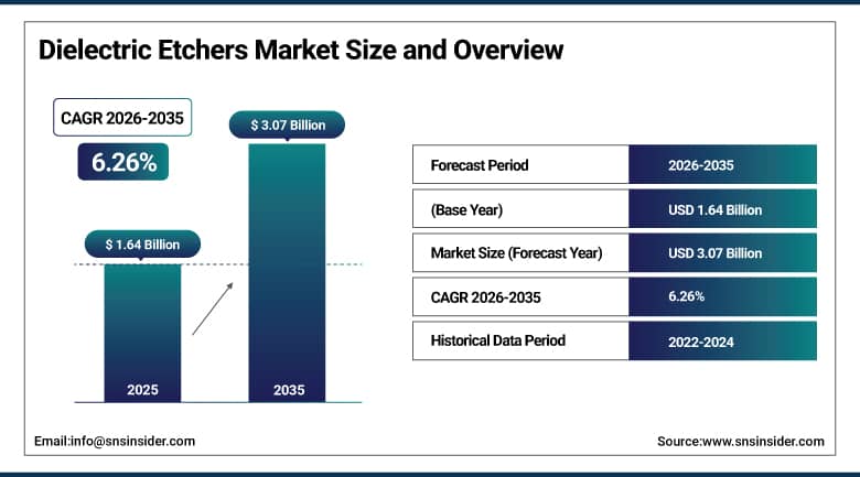
The Dielectric Etchers Market size was valued at USD 1.64 billion in 2025 and is expected to reach USD 3.07 billion by 2035, growing at a CAGR of 6.26% from 2026-2035.
The Dielectric Etchers Market is witnessing steady growth As there is an increasing requirement for sophisticated semiconductor devices along with the miniaturization of the electronic components. The trend towards the development of the smaller nodes and sophisticated architecture requires the application of highly accurate and selective etching techniques of dielectric. The increase in the production of the logic, memory, and advanced integrated circuits will support the growth of the market. Moreover, the rise in the investments in the fabrication plants, advanced packaging techniques and applications like artificial intelligence, high performance computing, 5G, etc. will also contribute to the growth of the market.
In 2025, TSMC reported that 7-nm and more advanced technologies accounted for 74% of total wafer revenue, up from 69% in 2024, highlighting continued growth in advanced semiconductor manufacturing.
To Get More Information On Dielectric Etchers Market - Request Free Sample Report
Dielectric Etchers Market Trends:
-
Rising demand for advanced semiconductor devices is driving adoption of high-precision dielectric etching technologies for increasingly complex device architectures.
-
Increasing production of advanced logic and memory chips is expanding demand for precise etching solutions with improved selectivity and process control.
-
Growing investments in semiconductor fabrication facilities are accelerating deployment of advanced dielectric etching equipment across leading-edge manufacturing environments.
-
Advancements in plasma-based etching technologies are improving etch uniformity, selectivity, feature control, and performance across complex wafer structures.
-
Increasing adoption of three-dimensional device architectures is creating demand for highly controlled dielectric etching processes capable of producing deeper and narrower features.
U.S. Dielectric Etchers Market Size Outlook:
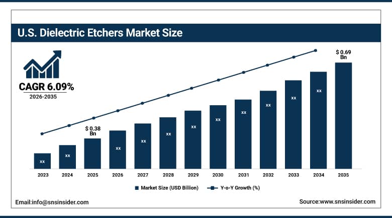
The U.S. Dielectric Etchers Market was valued at USD 0.38 billion in 2025 and is expected to reach USD 0.69 billion by 2035, growing at a CAGR of 6.09% from 2026-2035.
The U.S. Dielectric Etchers Market is experiencing steady growth as a result of the growing production of semiconductors and rising demand for state-of-the-art electronic components. The ongoing innovation in process technology and the design of semiconductor devices has led to the increasing demand for dielectric etching technologies that are more accurate and selective. The increase in the production of logic, memory, and advanced ICs is fueling market demand. Moreover, increased capital investment in the domestic production of semiconductor chips, along with rising uses in artificial intelligence, supercomputers, and 5G, has been helping the market grow. The continuous innovation in plasma etching techniques has increased production efficiency.
In 2025, Micron announced approximately US$200 billion in planned U.S. manufacturing and R&D investment, including leading-edge DRAM and HBM production to support growing AI-driven semiconductor demand.
Dielectric Etchers Market Segment Analysis:
-
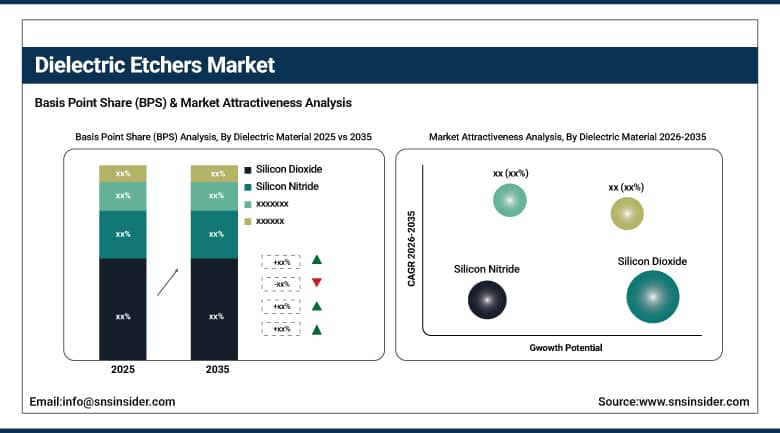
By Dielectric Material, Silicon Dioxide dominated the Dielectric Etchers Market with 46% share in 2025; Silicon Nitride is expected to grow at the fastest CAGR of 7.19% from 2026–2035.
-
By Technology, Reactive Ion Etching dominated the Dielectric Etchers Market with the highest revenue share in 2025; Inductively Coupled Plasma Etching is expected to grow at the fastest CAGR from 2026–2035.
-
By Wafer Size, 300 mm dominated the Dielectric Etchers Market with 64% share in 2025; 300 mm is expected to grow at the fastest CAGR of 6.76% from 2026–2035.
-
By End User, Pure-Play Foundries dominated the Dielectric Etchers Market with 41% share in 2025; Integrated Device Manufacturers (IDMs) are expected to grow at the fastest CAGR of 7.20% from 2026–2035.
By Dielectric Material, Silicon Dioxide dominates the dielectric etchers market, Silicon Nitride grows fastest.
Silicon Dioxide segment dominated the Dielectric Etchers Market with the highest revenue share of about 46% in 2025 Because of its wide use in semiconductor manufacturing, good dielectric properties, process compatibility, and reliable etching capabilities. Its wide usage in logic devices, memory, and integrated circuits, backed by well-developed manufacturing techniques and industrial acceptance, further strengthened its dominant position in the market.
Silicon Nitride segment is expected to grow at the fastest CAGR of 7.19% from 2026-2035 Due to growing requirements of sophisticated semiconductor devices that need better dielectric isolation and thermal as well as electrical properties. With growing applications in memory, logic, and power devices, and rising production of complex structures, further investment in the semiconductor industry is anticipated to drive the segment’s growth.
By Technology, Inductively Coupled Plasma Etching dominates the dielectric etchers market and grows fastest.
Inductively Coupled Plasma Etching segment dominated the Dielectric Etchers Market with the highest revenue share of about 43% in 2025 due to its high accuracy in etching, good process control, and the capability to create high aspect ratio features. Its popularity in advanced semiconductor processing, suitability for challenging dielectrics, and consistent performance in production operations made it the leading product in the market.
Inductively Coupled Plasma Etching segment is expected to grow at the fastest CAGR of 7.16% from 2026-2035 As a result of increasing demand for accurate etching of complicated semiconductor structures. The better selectivity, control, and capability of supporting smaller process geometries are pushing the use of this product in logic and memory production, and more fabrication capacity investments will boost segment growth.
By Wafer Size, 300 mm dominates the dielectric etchers market and grows fastest.
300 mm segment dominated the Dielectric Etchers Market with the highest revenue share of about 64% in 2025 This is due to its wide adoption in large-scale semiconductor production and better wafer-level productivity. Higher wafer sizes mean that more devices can be made per cycle, thus making the manufacturing process efficient and economical. There was also good demand for the company from logic and memory fabs.
300 mm segment is expected to grow at the fastest CAGR of 6.76% from 2026-2035 because of the ongoing growth in advanced semiconductor manufacturing and growing needs for high volume manufacturing. Investments in new fab construction, capacity growth, and production of advanced logic and memory chips are promoting the use of 300 mm wafer fabs, based on higher efficiency and economics of scale.
By End User, Pure-Play Foundries dominate the dielectric etchers market, Integrated Device Manufacturers (IDMs) grow fastest.
Pure-Play Foundries segment dominated the Dielectric Etchers Market with the highest revenue share of about 41% in 2025 as a result of growing trends toward outsourcing in semiconductor fabrication along with increased demands from fabless chip design companies. The emphasis that such companies put on manufacturing in large volumes, using advanced processes and serving different customers creates the need for dielectric etching tools. Further capacity increases only reinforced their market position.
Integrated Device Manufacturers (IDMs) segment is expected to grow at the fastest CAGR of 7.20% from 2026-2035 in connection with rising tendencies towards the outsourcing of production in semiconductor industry along with greater expectations of fabless chip design manufacturers. The focus that is made by such manufacturers on mass production through employing advanced technology and targeting at various consumers leads to the creation of demand for dielectric etching equipment. Additional capacity became only an extra market factor.
Regional Analysis:
|
Region |
Major Country |
Share within Region, 2025 (%) |
|---|---|---|
|
North America |
United States |
89.0% |
|
Europe |
Germany |
28.0% |
|
Asia Pacific |
China |
31.5% |
|
Middle East & Africa |
UAE |
23.0% |
|
Latin America |
Brazil |
40.5% |
Asia Pacific Dielectric Etchers Market Insights
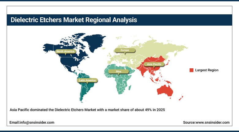
Asia Pacific dominated the Dielectric Etchers Market with a market share of about 49% in 2025, supported by its strong semiconductor manufacturing base, advanced fabrication investments, and growing production of memory and logic chips. The region is also expected to grow at the fastest CAGR of about 6.93% from 2026–2035, driven by expanding semiconductor capacity, advanced process nodes, AI demand, and government-supported chip manufacturing initiatives.
The China Dielectric Etchers Market accounted for a market share of 31.5%, This is due to the fast expansion of the semiconductor manufacturing industry and increased investments in the development of advanced wafer manufacturing plants. The growth in the production of memory, logic, and advanced chips for AI, consumer electronics, automotive technology, and data centers is contributing to the increased demand for dielectric etchers. Government backing for local development of semiconductors, increasing fabrication capabilities, and technological developments are making things even better in China.
Get Customized Report as Per Your Business Requirement - Enquiry Now
North America Dielectric Etchers Market Insights
North America Dielectric Etchers Market is witnessing steady growth, in relation to the trends in the rise of the outsourcing of manufacturing processes within the semiconductor industry and also the high expectations from the side of fabless chip manufacturers. The attention paid to the mass production using the most advanced technologies and addressing different categories of consumers results in the emergence of the demand for dielectric etching equipment. The additional capacity is just another market factor
The U.S. Dielectric Etchers Market accounted for a market share of 89.0%, backed up by robust semiconductor manufacturing infrastructure and rising investment in cutting-edge fab facilities. The growing requirement for complex integrated circuits in applications such as artificial intelligence, supercomputing, automotive electronic systems, and data centers is contributing to the growth of dielectric etching technology. Along with this, government initiatives for local semiconductor manufacturing, rising R&D initiatives, technology innovations, and investments in advanced node process technologies are aiding in the growth of dielectric etchers market in the US.
Europe Dielectric Etchers Market Insights
Europe Dielectric Etchers Market is experiencing steady growth, With support from strong semiconductor manufacturing infrastructure and increasing investments in state-of-the-art fabrication plants. The increasing demand for complex integrated circuits in areas like artificial intelligence, supercomputing, automotive electronics, and data centers has helped drive dielectric etching technology. Besides this, initiatives taken by the government towards localized semiconductor manufacturing, R&D activities, advancements in technology, and advanced node process technologies have been aiding the growth of dielectric etchers market in the US.
The Germany Dielectric Etchers Market accounted for a market share of 28.0%, backed by the presence of an efficient semiconductor and electronic manufacturing industry and increased investments in sophisticated fabrication technology. The growing need for automotive electronics, industrial components, and high-end computing has led to the adoption of precise dielectric etching machines. Germany’s emphasis on innovative semiconductor technology, research, development, and improving its domestic chip manufacturing capability has fueled growth in the market and increased demand for dielectric etchers in the country.
Middle East & Africa and Latin America Dielectric Etchers Market Insights
The Middle East & Africa and Latin America Dielectric Etchers Market is gradually expanding, This is because of the rapid growth in the manufacture of semiconductors industry and also the investments made on the production of advanced wafer factories. The growth in manufacturing of memory, logic and also advanced chips used in AI, consumer electronics, automotive technology and data center is causing the increase in the need for dielectric etchers. The support from the government for the development of semiconductors locally, along with the technological advancements, is making things better in China.
The UAE Dielectric Etchers Market accounted for a market share of 23.0%, backed by the rise in investments in technology infrastructure, semiconductor activities, and high-tech manufacturing. The increase in the need for electronic devices and digital technologies provides opportunities for dielectric etch equipment in the UAE. Efforts taken by the government to diversify its economy and modernize its industries will help in adopting dielectric etching machines.
Market Dynamics:
Growth Drivers: Increasing semiconductor miniaturization and advanced process nodes are accelerating demand for highly precise dielectric etching technologies
Increasing semiconductor miniaturization is significantly driving demand for dielectric etchers as chip manufacturers move toward smaller process nodes and increasingly complex device architectures. Highly logical and memory-based systems use etching of dielectric substances like silicon dioxide and silicon nitride to form nanostructures that are highly accurate in their dimensions. Dielectric etching offers improvements in selectivity, profile, and uniformity control. These features are important in sustaining wafer yield and device performance. The emergence of production of AI processors, high-performance computer chips, advanced memory, and consumer electronic products is driving demand for semiconductor equipment. Increasing complexity of the processes due to 3D and multi-layer formation is motivating semiconductor companies to invest in highly-controlled dielectric etching.
Restraints: High equipment costs and complex process requirements can limit adoption of advanced dielectric etching systems globally
High equipment costs represent a significant challenge for the Dielectric Etchers Market. Advanced dielectric etching systems incorporate sophisticated plasma sources, vacuum technologies, process-control systems, and precision components that require substantial capital investment. Logic and memory-oriented systems utilize dielectric etching of materials such as silicon dioxide and silicon nitride to create highly precise nanostructures. Some of the benefits brought about by dielectric etching include selectivity, profile, and uniformity control. These attributes are crucial in maintaining wafer yield and performance. The rising demand for the manufacture of AI processors, high-end computer chips, advanced memory, and consumer electronics is pushing the growth in semiconductor equipment. This is being driven by growing process complexity from the 3D and multi-layer creation process.
Opportunities: Expansion of advanced logic and memory manufacturing creates significant opportunities for next-generation dielectric etching equipment
Growing production of advanced logic and memory devices is creating significant opportunities for dielectric etcher manufacturers. Modern semiconductor architectures increasingly incorporate complex structures such as gate-all-around transistors, advanced interconnects, three-dimensional memory, and high-aspect-ratio features. Such systems need extremely accurate dielectric etch processing with better selectivity, profile control, and reduced process damage. The increased market need for artificial intelligence accelerators, high-performance microprocessors, advanced DRAMs, and NAND chips is prompting semiconductor makers to increase their capacity to produce advanced devices. Tool makers with advanced plasma processes, improved process control, and advanced material handling techniques for ever more difficult dielectrics could take advantage of this trend. Future semiconductor scaling is forecast to drive future demand for next-generation dielectric etch systems.
Recent Developments:
-
Applied Materials introduced new selective etch technology designed for increasingly deep and narrow 3D logic and memory structures, supporting precision processing for next-generation AI chips and advanced semiconductor manufacturing.
-
Oxford Instruments expanded its plasma-processing capabilities, including atomic-layer etch technology, supporting advanced semiconductor, compound-semiconductor, and quantum applications requiring precise low-damage material removal.
-
Lam Research introduced Akara®, an advanced plasma etch system providing enhanced plasma control and precision for challenging 3D semiconductor structures and next-generation device scaling.
-
Hitachi High-Tech launched the DCR Etch System 9060 Series, enabling atomic-level isotropic dry etching for high-aspect-ratio 3D semiconductor structures while improving precision, throughput, and productivity.
Dielectric Etchers Companies are:
-
Lam Research Corporation
-
Tokyo Electron Limited
-
Hitachi High-Tech Corporation
-
Mattson Technology, Inc.
-
ASM International N.V.
-
NAURA Technology Group Co., Ltd.
-
Advanced Micro-Fabrication Equipment Inc. (AMEC)
-
KLA Corporation (SPTS Technologies)
-
Oxford Instruments plc
-
Plasma-Therm LLC
-
ULVAC, Inc.
-
SAMCO Inc.
-
Veeco Instruments Inc.
-
Nordson Corporation (Nordson MARCH)
-
Corial SAS
-
Trion Technology, Inc.
-
Plasma Etch, Inc.
-
SEMES Co., Ltd.
Dielectric Etchers Market Report Scope:
| Report Attributes | Details |
|---|---|
| Market Size in 2025 | USD 1.64 Billion |
| Market Size by 2035 | USD 3.07 Billion |
| CAGR | CAGR of 6.26% From 2026 to 2035 |
| Base Year | 2025 |
| Forecast Period | 2026-2035 |
| Historical Data | 2022-2024 |
| Report Scope & Coverage | Market Size, Segments Analysis, Competitive Landscape, Regional Analysis, DROC & SWOT Analysis, Forecast Outlook |
| Key Segments | • By Dielectric Material (Silicon Dioxide, Silicon Nitride, Other Dielectric Materials) • By Technology (Reactive Ion Etching, Inductively Coupled Plasma Etching, Electron Cyclotron Resonance Etching, Vapor Phase Etching, Other Technologies) • By Wafer Size (Less Than 150 mm, 200 mm, 300 mm, Other Wafer Sizes) • By End User (Pure-Play Foundries, Integrated Device Manufacturers (IDMs), MEMS & Sensor Fabs, R&D and Pilot Lines, Other End Users) |
| Regional Analysis/Coverage | North America (US, Canada), Europe (Germany, UK, France, Italy, Spain, Russia, Poland, Rest of Europe), Asia Pacific (China, India, Japan, South Korea, Australia, ASEAN Countries, Rest of Asia Pacific), Middle East & Africa (UAE, Saudi Arabia, Qatar, South Africa, Rest of Middle East & Africa), Latin America (Brazil, Argentina, Mexico, Colombia, Rest of Latin America). |
| Company Profiles | Applied Materials, Inc., Lam Research Corporation, Tokyo Electron Limited, Hitachi High-Tech Corporation, Mattson Technology, Inc., ASM International N.V., NAURA Technology Group Co., Ltd., Advanced Micro-Fabrication Equipment Inc. (AMEC), KLA Corporation (SPTS Technologies), Oxford Instruments plc, Plasma-Therm LLC, ULVAC, Inc., SAMCO Inc., Veeco Instruments Inc., Nordson Corporation (Nordson MARCH), Corial SAS, Trion Technology, Inc., Plasma Etch, Inc., SEMES Co., Ltd., and Jusung Engineering Co., Ltd. |
Frequently Asked Questions
The Dielectric Etchers Market is expected to grow at a CAGR of 6.26% from 2026 to 2035.
The Dielectric Etchers Market was valued at USD 1.64 billion in 2025.
Increasing demand for advanced semiconductor devices and miniaturized integrated circuits is driving dielectric etcher adoption, requiring precise, high-aspect-ratio etching for advanced node fabrication.
The Silicon Dioxide segment dominated the Dielectric Etchers Market in 2025.
Asia Pacific dominated the Dielectric Etchers Market in 2025.
