Optical Metasurface Market Report Scope & Overview:
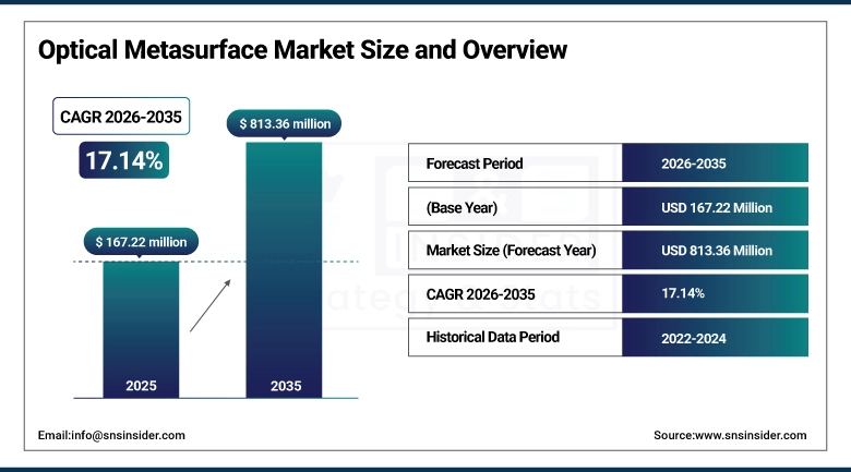
The Optical Metasurface Market size was valued at USD 167.22 Million in 2025 and is projected to reach USD 813.36 Million by 2035, growing at a CAGR of 17.14%during 2026–2035.
The Optical Metasurface market driven by the application of artificial intelligence in design and optimization techniques Inversion design, surrogate modeling, and AI-driven reinforcement learning are improving the upper limits for performance of unit-cells while allowing nanophotonic devices to integrate into systems unimpeded by their complexity. This development is contributing to a scalable, accurate, and efficient optical system. Demand is increasing because industry verticals like imaging, AR/VR, LiDAR, and computational optics need high performance photonic solutions at a small form factor. As adoption of intelligent design frameworks continues to grow, it helps speed up the process of innovation, reduce turnaround time and enable a transition to new age smart optical technologies across the globe.
In Dec 2025, Seamless Unit-Cell Design in an AI-Driven Optical Metasurface Facilitates Faster Development of Nanophotonic Devices with System-Level Integration in Dec 2025 Surrogate Modeling, Inverse Design & Reinforcement learning based approach to design for performance in imaging, AR/VR/LiDAR and computational optics.
Optical Metasurface Market Size and Growth Forecast:
-
Market Size in 2025: USD 167.22 Million
-
Market Size by 2035: USD 813.36 Million
-
CAGR: 17.14% (from 2026 to 2035)
-
Base Year: 2025
-
Forecast Period: 2026–2035
-
Historical Data: 2022–2024
To Get more information on Optical Metasurface Market - Request Free Sample Report
Optical Metasurface Market Trends Highlights:
-
Increasing adoption in quantum computing, LiDAR, AR/VR, and advanced imaging applications
-
Strong integration with AI-driven design techniques such as inverse design and reinforcement learning
-
Shift from bulky optical components to compact, planar nanostructured surfaces
-
Rising use in consumer electronics, defense, healthcare imaging, and telecommunications
-
Advancements in CMOS-compatible fabrication enabling scalable mass production
-
Expanding research in tunable and reconfigurable metasurfaces for dynamic optical control
-
Growing investments in semiconductor photonics and next-generation optical technologies worldwide
U.S. Optical Metasurface Market Size Outlook:
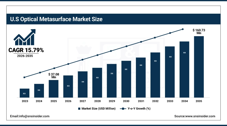
The U.S. Optical Metasurface Market size was valued at USD 37.08 Million in 2025 and is projected to reach USD 160.73 Million by 2035, growing at a CAGR of 15.79%during 2026–2035, The demand is fueled by increasing adoption in quantum computing, LiDAR, defense optics, and AR/VR applications that rely on high-precision and compact light control. Increased investments in photonics for silicon and, in particular, continuous advances in CMOS-compatible manufacturing methods are other trends speeding up market growth in the US.
Optical Metasurface Market Drivers:
-
Optical Metasurface Market Growth Drivers and Emerging Trends
The optical metasurface is projected to witness grow at a rapid rate across the globe, primarily due to the faster increase in demand for ultra-compact, energy-efficient and high-performance photonic systems. Metasurfaces are becoming increasingly popular with demand from quantum computing and LiDAR, AR/VR, and advanced imaging applications, which require controlled manipulation of light at nanoscale resolution. Following improvements from integration to CMOS-compatible manufacturing processes for large-scale production, reconfigurable and tunable metasurfaces, and development of AI-embedded optical computing systems are next on the list. In addition, high investments accelerate the rapid innovation over semiconductor photonics and miniaturized optical devices from this background. The advancements listed above really make the positioning of metasurfaces as a universal enabling technology for emerging communication, sensing and computational platforms worldwide possible.
12 Feb 2026 — optical metasurface technology enables passive intensity-based optical image filtering using silicon nanostructures for more efficient machine vision and AI diagnostics.This approach improves optical nonlinearity at low energy levels, allowing advanced image feature extraction and supporting low-power optical neural networks and smart imaging systems.
Optical Metasurface Market Restraints:
-
Key Barriers to Adoption in Optical Metasurface Technology
The optical metasurface market has low penetration and therefore highly restrained market This high fabrication complexity and the nanoscale precision needed makes the production technically challenging and cost prohibitive. The high costs of advanced lithography and specialized materials increase total manufacturing cost and limit otheir the scalability for mass-market applications. However, performance drawbacks such as efficiency roll-off at specific wavelengths negatively impact performance of some optic systems. At the same time, it hinders commercialization, because there are no global standards and there is no large-scale manufacturing infrastructure. Advanced semiconductor ecosystems impose further limitation for adoption in developing regions, presenting hurdle on the heel of technological promise for global proliferation.
Optical Metasurface Market Opportunities:
-
Optical Metasurfaces Driving Next-Generation Photonics and Quantum Innovation
The Optics Metasurface with Cold, Compact, Efficient Optical Device Performance Optics metasurfaces are gaining high market growth due to the high need for miniaturization and efficiency coupled with high accuracy in optical devices. Scalable, low-cost production stalled commercialization in many sectors due to non CMOS compatible manufacturing. That's ramping up uptake of the tech alongside rising spending on photonics and quantum technologies by replacing bulky optical components with ultra-thin flat devices, metasurfaces are opening up new applications from aerospace/defense to health care diagnostics to next generation consumer electronics ecosystems globally.
In Mar 2026, Optical metasurface technology allows researchers in China to trap densities of up to 78,400 neutral atoms many more than the ~ 10,000 trap limit of traditional SLM and AOD systems for quantum computing applications. This is a metasurface optimized using a weighted Gerchberg–Saxton algorithm and fabricated with CMOS-compatible processes that enable scalability to large neutral-atom quantum computers.
Optical Metasurface Market Segment Highlights:
-
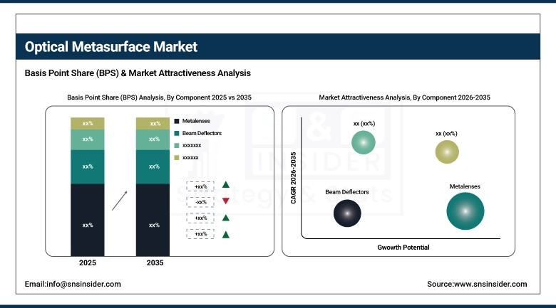
By Component: Dominant – Metalenses (37.20% in 2025 → 34.50% in 2035); Fastest Growing – Beam Deflectors (18.50% in 2025 → 24.80% in 2035
-
By Material: Dominant – Dielectric Metasurfaces (50.50% in 2025 → 44.00% in 2035); Fastest Growing – Hybrid Metasurfaces (22.00% in 2025 → 34.00% in 2035)
-
By Application: Dominant – AR & VR (28.40% in 2025 → 31.60% in 2035); Fastest Growing – Optical Communication (22.20% in 2025 → 23.80% in 2035)
-
By End Use: Dominant – Commercial (63.00% in 2025 → 71.00% in 2035); Fastest Growing – Industrial (18.20% in 2025 → 19.80% in 2035)
By Component: Metalenses (Dominant) and Beam Deflectors (Fastest-Growing)
Metalenses hold the largest market share due to their superior focusing efficiency, compact flat-optics structure, and extensive use in imaging systems, AR/VR devices, and advanced optical applications. However, Beam Deflectors are the fastest expanding segment thanks to their ability for highly accurate and agile light Steering, and thus aid in the rapid commercialization of LiDAR, optical communication, and sensing technologies that are supported by the demand for High-Speed, compact, and reconfigurable Photonic solutions.
By Material: Dielectric Metasurfaces (Dominant) and Hybrid Metasurfaces (Fastest-Growing)
Dielectric Metasurfaces hold the largest market share due to their high efficiency, low optical loss, and strong performance in imaging and photonic applications. However, Hybrid Metasurfaces segment is witnessing the highest CAGR growth in types as the combination of dielectric and metallic features, which make it can provide more tunable, and operate on a wider wavelength range for both active and passive next-generation optical systems.
By Application: AR & VR (Dominant) and Optical Communication (Fastest-Growing)
AR & VR dominate the market due to rising adoption in immersive displays, smart devices, and advanced visualization technologies. However, Optical Communication due to vibrant demand for greater speed records on a chip, compact optical components, and new generation 5G/6G community infrastructure.
By End Use: Commercial (Dominant) and Industrial (Fastest-Growing)
Commercial accounts for the highest share in the end-use segment since optical metasurface for commercial application is generally used in consumer electronics, imaging systems, and telecommunications. On the other hand, Industrial is expected to be the fastest-growing segment as proliferation in automation, sensing, LiDAR systems, and advanced manufacturing technologies necessitating high-precision optical control.
Optical Metasurface Market Regional Highlights:
-
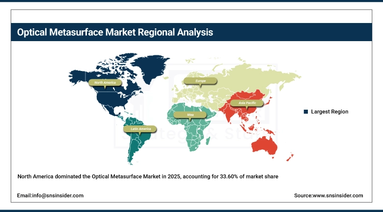
North America (Dominating – 33.60% in 2025 → 30.40% in 2035, CAGR 15.97%)
-
Asia-Pacific (Fastest Growing – 31.00% in 2025 → 39.00% in 2035, CAGR 19.83%)
-
Europe (27.40% in 2025 → 22.60% in 2035, CAGR 14.89%)
-
South America (3.90% in 2025 → 3.10% in 2035, CAGR 14.45%)
-
Middle East & Africa (4.10% in 2025 → 4.90% in 2035, CAGR 19.23%)
North America Optical Metasurface Market Insights:
North America is expected to remain the largest regional market in the optical metasurface industry over the forecast period, driven by strong investments in advanced photonics, defense optics, and semiconductor innovation. The region benefits from the presence of leading technology companies, robust R&D infrastructure, and early adoption of metasurface-based applications in imaging, sensing, and AR/VR systems, which collectively reinforce its dominant position and sustained growth outlook through the forecast horizon.
Get Customized Report as per Your Business Requirement - Enquiry Now
U.S. Optical Metasurface Market Insights:
The United States optical metasurface market is rapidly growing and dominant due to strong R&D, advanced photonics ecosystem, defence applications, and high adoption in AR/VR and imaging technologies.
Asia-Pacific Optical Metasurface Market Insights:
Asia Pacific is currently the fastest growing region in the optical metasurface market, driven by rapid industrialization, expanding semiconductor manufacturing, and increasing investments in advanced photonics and optoelectronics. Countries such as China, Japan, South Korea, and India are significantly contributing to market expansion through strong government support, rising R&D activities, and growing adoption of metasurface technologies in consumer electronics, telecommunications, and imaging applications. The region’s large manufacturing base and accelerating technological advancements further reinforce its position as the fastest-growing market globally.
China Optical Metasurface Market Insights:
China is a key driver and dominant force in the optical metasurface market, supported by massive investments in photonics, strong semiconductor manufacturing capabilities, and rapid expansion of advanced imaging and communication technologies.
Europe Optical Metasurface Market Insights:
The Europe optical metasurface market is expected to grow steadily, driven by robust research activities, improved photonics development, and rising deployment across automotive sensing, aerospace and healthcare imaging applications. Well-developed academia–industry collaboration and state-of-the-art nanophotonic and optical engineering offer a great advantage to the region. The increase in demand for applications of high-precision optical systems and growing investments in next-gen imaging technologies will also accelerate the continuous expansion revenue of the market across Europe.
Germany Optical Metasurface Market Insights:
Germany is one of the leading markets for optical metasurfaces in Europe fueled by its robust industrial roots, engineering prowess, and significant adoption in automotive optics, aerospace systems, and imaging technologies.
Latin America Optical Metasurface Market Insights:
The Latin America optical metasurface market is showing gradual growth, driven by increasing adoption of advanced optical technologies in telecommunications, industrial inspection, and academic research. Rising investments in photonics infrastructure and expanding awareness of next-generation imaging and sensing solutions are further supporting market development across the region.
Brazil Optical Metasurface Market Insights:
The Brazil optical metasurface market will grow with a healthy growth rate in the region, owing to rising research activities in photonics, increasing deployment of advanced imaging technologies and expanding applications in telecommunications and industrial inspection systems.
Middle East & Africa Optical Metasurface Market Insights:
The Middle East & Africa optical metasurface market is gaining max impetuses with more investments for advanced optical technologies, an uptick in demand for the optical metasurf, high-precision imaging & sensing and defense & surveillance systems. The gradual enhancement of research capabilities by countries across the region and collaboration with global technology providers is supporting the penetration of metasurface-based applications across the telecommunication, healthcare, and industrial sectors.
United Arab Emirates (UAE) Optical Metasurface Market Insights:
The Middle East & Africa optical metasurface market is expanding steadily, with the United Arab Emirates emerging as the dominant country in the region due to its strong investments in advanced defense systems, smart city initiatives, and rapid adoption of cutting-edge optical and photonics technologies. The country’s focus on innovation, along with growing applications in surveillance, telecommunications, and high-precision imaging, is significantly driving regional market growth.
Optical Metasurface Market Competitive Landscape:
Metalenz is an optical metasurface company originally spun out of Harvard University in 2016 and focused on developing metalens-based imaging and sensing solutions for consumer electronics and other high-performance optical systems. It specializes in miniaturized 3D depth sensing, polarization imaging and biometrics with more than 150 patents in the areas of metasurface design and manufacturing, along with full-stack optical systems. Key to commercialization of metasurface technology for AR/VR, smartphones, and next-generation imaging applications.
-
In August 2025, Metalenz expanded its metasurface portfolio into system-level sensing applications, including secure biometrics and advanced 3D imaging solutions. The company strengthened its leadership with over 150 patents supporting compact depth sensing and polarization-based imaging technologies.
Lumotive is a matured optical semiconductor company that leverages its proprietary Light Control Metasurface (LCM) technology for solid-state beam steering in LiDARs. By substitute mechanical scanning with programmable optical metasurfaces, compact, stable, and high-performance 3D sensing solutions for robotics, automotive and industrial automation can be realized.
Hokuyo Automatic Co., Ltd. Founded in 1946, Hokuyo Automatic Co., Ltd. is a Japan-based industrial sensor and automation company that manufactures LiDAR and related detection equipment for robotics, logistics, and factory automation. The firm focuses on high-precision safety sensors and scanning technologies that support autonomous navigation, industrial safety, and automation efficiencies in manufacturing markets around the world.
-
In May 2024, Lumotive and Hokuyo jointly launched the YLM-10LX, the world’s first commercial 3D LiDAR sensor using true solid-state optical beam steering based on Lumotive’s Light Control Metasurface (LCM) technology. The system eliminates mechanical scanning parts, enabling more stable, programmable, and high-performance 3D sensing for industrial automation and robotics applications.
Optical Metasurface Companies are:
-
STMicroelectronics
-
Moxtek
-
MetaOptics Technologies
-
NIL Technology (NILT)
-
2Pi Optics
-
Tunoptix
-
Kymeta Corporation
-
Viavi Solutions
-
Coherent Corp
-
Hamamatsu Photonics
-
Jenoptik
-
Thorlabs
-
Lumentum
-
II-VI Incorporated (Coherent)
-
Broadcom Inc. (Optical Solutions)
-
Intel Corporation (Photonics Division)
-
Sony Semiconductor Solutions
-
Carl Zeiss AG
| Report Attributes | Details |
|---|---|
| Market Size in 2025 | USD 167.22 Million |
| Market Size by 2035 | USD 813.36 Million |
| CAGR | CAGR of 17.14% From 2026 to 2035 |
| Base Year | 2025 |
| Forecast Period | 2026-2035 |
| Historical Data | 2022-2024 |
| Report Scope & Coverage | Market Size, Segments Analysis, Competitive Landscape, Regional Analysis, DROC & SWOT Analysis, Forecast Outlook |
| Key Segments | • By Component(Metalenses, Beam Deflectors, Polarization Converters, Meta-Holograms and Others) • By Material (Dielectric Metasurfaces, Metallic Metasurfaces and Hybrid Metasurfaces) • By Application(AR & VR, Optical Communication, Imaging & Sensing Sys, Holography, Sensing & Detection and Others) • By End Use(Commercial, Industrial, Research & Academia and Others) |
| Regional Analysis/Coverage | North America (US, Canada), Europe (Germany, UK, France, Italy, Spain, Russia, Poland, Rest of Europe), Asia Pacific (China, India, Japan, South Korea, Australia, ASEAN Countries, Rest of Asia Pacific), Middle East & Africa (UAE, Saudi Arabia, Qatar, South Africa, Rest of Middle East & Africa), Latin America (Brazil, Argentina, Mexico, Colombia, Rest of Latin America). |
| Company Profiles | Metalenz, STMicroelectronics, Moxtek, MetaOptics Technologies, NIL Technology (NILT), Lumotive, 2Pi Optics, Tunoptix, Kymeta Corporation, Viavi Solutions, Coherent Corp, Hamamatsu Photonics, Jenoptik, Thorlabs, Lumentum, II-VI Incorporated (Coherent), Broadcom Inc. (Optical Solutions), Intel Corporation (Photonics Division), Sony Semiconductor Solutions, Carl Zeiss AG. |
Frequently Asked Questions
North America dominated the Optical Metasurface Market in 2025.
The “Metalenses” segment dominated during the projected period.
The key drivers of the optical metasurface market include rising demand for compact photonic systems, growth in quantum computing, LiDAR and AR/VR applications, and advancements in AI-driven design and CMOS-compatible fabrication.
The Market was valued at USD 167.22 Million in 2025 and is projected to reach USD 813.36 Million by 2035.
The Market is expected to grow at a CAGR of 17.14%during 2026–2035.
Get in Touch
