Power GaN Device Market Report Scope & Overview:
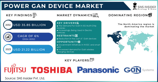
The Power GaN device market size was valued at USD 21.22 Billion in 2023 and is expected to grow to USD 35.85 Billion by 2032 and grow at a CAGR Of 6% over the forecast period of 2024-2032.
The market is divided into GaN power discrete devices, GaN power ICs, and GaN power modules depending on the kind of device.
The device, application, and geographic segments are used to divide the market for GaN power devices. Due to its capacity to fabricate more compact devices for a given resistance value and breakdown voltage as compared to silicon devices, gallium nitride (GaN) transistors have emerged as a higher-performing alternative to silicon-based transistors. Extremely low resistance and high-frequency switching are both achievable with these power devices. High-efficiency power supply, electric vehicles (EV), hybrid electric vehicles (HEV), solar inverters, and RF switching all make use of these qualities. Additionally, these devices can be used to power servers, IT equipment, high-efficiency & reliable power sources, as well as EV & HEV devices. As a result, the market for GaN power devices is influenced by rising applications.
Power GaN Device Market Size and Forecast
-
Market Size in 2023: USD 21.22 Billion
-
Market Size by 2032: USD 35.85 Billion
-
CAGR: 6.0% from 2024 to 2032
-
Base Year: 2023
-
Forecast Period: 2024–2032
-
Historical Data: 2022–2023
Get more information on Power GaN Device Market - Request Sample Report
Power GaN Device Market Trends:
-
Rapid adoption in fast-charging consumer electronics is accelerating demand, with GaN chargers growing at over 25% CAGR, driven by higher efficiency and compact designs.
-
Expansion in data centers and telecom infrastructure is boosting deployment, as GaN devices deliver up to 40% lower power losses compared to traditional silicon MOSFETs.
-
Rising EV and onboard charger integration is strengthening market growth, with EV power electronics demand increasing at over 20% annually.
-
Increasing use in renewable energy inverters and solar applications is enhancing efficiency, with GaN enabling up to 3–5% higher system efficiency.
-
Advancements in high-voltage GaN technology (600V–1200V) are expanding industrial adoption, supporting 30% smaller system footprints and improved thermal performance.
MARKET DYNAMICS
KEY DRIVERS:
-
The Demand For GaN In 5G Multi-Chip Modules
-
Increasingly Being Used In Electric Vehicles
GaN devices are increasingly being used in electric vehicles because they can drive motors at greater voltages with less current leakage between the collector and emitter terminals and with higher switching rates. Furthermore, power management devices are needed for the high-voltage battery systems in both HEVs and EVs to handle the power from the battery to the motor drivers.
There is a rise in the deployment of GaN devices, which in turn fuels market expansion. Additionally, sales of electric vehicles have greatly surged recently and are projected to reach 41 million by 2040. It is anticipated that this will present a lucrative potential for market expansion.
RESTRAIN:
-
Reduction in the cost of GaN devices
The market trend for GaN power devices and their adoption is anticipated to be sped up across a variety of industry verticals. the large band gap of recently released GaN power transistors and modules provides SiC-like performance with significant cost savings. This cost reduction is possible because silicon substrates, which are more readily available and less expensive than SiC, may be used to develop GaN power devices. In comparison to silicon metal-oxide-semiconductor field-effect transistors (MOSFETs) and insulated-gate bipolar transistors (IGBTS), GaN-on-silicon devices are anticipated to have performance that is on par with or even better than those technologies.
OPPORTUNITY:
-
Government Initiatives in HVDC and smart grid
-
Increased demand for GaN wireless charging devices
WiTricity Corp., a wireless charging firm, used a GaN field effect transistor (FET) to demonstrate wireless charging. In comparison to silicon MOSFETs, the switching speed of GAN FETs enables higher efficiency of resonant wireless power transfer. Because silicon-based power MOSFETs approach the upper limit of their switching capacity at higher frequencies, their operation is constrained. GaN power devices are employed in wireless charging applications because they have a very high switching capability. Concerning the carrier frequency in resonant transfer, GaN transistors are superior. This enables them to transfer power over long distances in a variety of consumer, medical, industrial, and automotive applications. Consequently, enhancing the Another element that boosts the demand for GaN devices is their falling cost.
CHALLENGES:
-
Maintaining the Standardization
-
Manufacturing Complexibility
Power GaN devices must be manufactured using specialized techniques that are more difficult and complex than those used to make silicon-based devices. Costs have increased as a result of the existing reduced manufacturing yield rates. For Power GaN devices to be used more widely, it is essential to develop effective production processes and boost yield rates.
IMPACT OF RUSSIAN UKRAINE WAR
The Russia-Ukrainian war caused significant disruptions throughout the automotive value chain and forced OEMs and suppliers to postpone or halt business with Russia. Due to a shortage of parts from Ukrainian suppliers, some OEMs in Europe and Eastern Europe have stopped or reduced their production.
The conflict between Russia and Ukraine has wide-ranging effects, and one sector of the tech sector where these effects are most noticeable is GaN (Gallium Nitride) devices. These devices, which improve power management system efficiency, have recently received a lot of attention. Unfortunately, the Russian-Ukrainian conflict has disrupted supply networks and production procedures, limiting the availability of materials essential for these devices. Lack of raw materials is a problem for companies who make these gadgets, and this has an impact on their capacity to innovate and advance past developments. This will probably have long-term implications on technological advancement, which will impede our efforts to move towards more ecologically friendly energy sources.
IMPACT OF ONGOING RECESSION
Individuals are becoming more frugal with their expenditures due to financial instability, which has diminished the market for technological equipment. On the other hand, as people and businesses look for methods to save expenses, there has been an increase in demand for energy-efficient items. GaN devices with great power density and efficiency are now being given more attention as a result of this. GaN technology is additionally more appealing than ever before due to its long-term sustainability advantages, especially in light of the subsidies and incentives that governments all over the world are providing for green energy programs. Consequently, we could be advantages of sustainability. Overall, it seems that GaN devices are still positioned to have a substantial impact on our future energy consumption patterns, although we may be temporarily facing a slowdown in consumer electronics purchases as a result of the recession.
KEY MARKET SEGMENTS:
By Product
-
GaN Radio Frequency Devices
-
Opto-semiconductors
By Component
-
Transistor
-
Diode
-
Rectifier
-
Power IC
-
Others
By Wafer Size
-
2-inch
-
4-inch
-
6-inch
-
8-inch
By End-use
-
Automotive
-
Consumer Electronics
-
Defense & Aerospace
-
Healthcare
-
Industrial & Power
-
Information & Communication Technology
-
Others
REGIONAL ANALYSIS
-
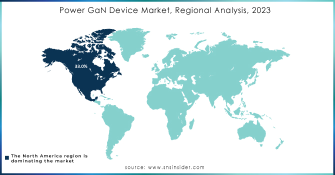
In 2022, the North American regional market dominated the industry and generated more than 33.0% of worldwide sales. The market expansion in the area is being fueled by the defense and aerospace industry's growing spending in R&D. Furthermore, it is anticipated that the business in the region will be driven by government support given to semiconductor companies. For instance, U.S. lawmakers proposed a plan in June 2020 to give semiconductor producers subsidies totaling more than USD 22.8 billion. The bill was designed to encourage the establishment of chip manufacturing in the United States.
-
The Asia Pacific regional market is to grow at the quickest rate during the projected period Rapid technological improvements are expected to enhance demand for high-performance and efficient radio frequency components. Some of the biggest producers of consumer electronics in the area, including LED display devices, cellphones, and gaming consoles, are nations like China and Japan.
Need any customization research on Power GaN Device Market - Enquiry Now
REGIONAL COVERAGE:
North America
-
USA
-
Canada
-
Mexico
Europe
-
Germany
-
UK
-
France
-
Italy
-
Spain
-
The Netherlands
-
Rest of Europe
Asia-Pacific
-
Japan
-
South Korea
-
China
-
India
-
Australia
-
Rest of Asia-Pacific
The Middle East & Africa
-
Israel
-
UAE
-
South Africa
-
Rest of the Middle East & Africa
Latin America
-
Brazil
-
Argentina
-
Rest of Latin American
KEY PLAYERS:
The major players are GaN Systems Inc., Toshiba Corporation, TAIWAN SEMICONDUCTOR MANUFACTURING COMPANY, LTD., Efficient Power Conversion Corporation Inc., FUJITSU Limited, ON SEMICONDUCTOR CORPORATION, PANASONIC CORPORATION, VISIC TECHNOLOGIES LTD, TEXAS INSTRUMENTS INC., Infineon Technologies AG and others are listed in a final report.
RECENT DEVELOPMENTS:
-
In September 2022, the introduction of the 100 V EFU2sU6, designed for 46 V UU-DU conversion used in high-density computing applications, 48 V BLDC motor drives for e-mobility and robotics, as well as solar optimizers and microinverters, and Class D Audio. Mode gallium nitride power FETs and ICs increase the variety of commercially available GaN.
-
Fujitsu Limited announced in September 2022 that it would be completely revamping its modernization services offerings (DX). Fujitsu will work with clients to visualize their present assets, such as business processes, data, applications, and IT infrastructure, to design a suitable DX platform. Additionally, it will help systems be modernized and made more efficient.
-
NXP Semiconductors N.V. revealed its upcoming 5G energy milestone in June 2021. The integration of 5G energy and Gallium Nitride technology into its multi-chip module architecture is being worked on, according to NXP Semiconductors N.V. Additionally, NXP unveiled RF solutions for 5G massive MIMO that combine GaN's high efficiency with multi-chip modules' compactness.
-
The world's most effective power-saving microwave power amplifier, which uses high-efficiency GaN-HEMT and lowers energy loss by 25%, was created by Fujitsu Limited in March 2021.
| Report Attributes | Details |
| Market Size in 2023 | US$ 21.22 Bn |
| Market Size by 2032 | US$ 35.85 Bn |
| CAGR | CAGR of 6 % From 2024 to 2032 |
| Base Year | 2023 |
| Forecast Period | 2024-2032 |
| Historical Data | 2020-2022 |
| Report Scope & Coverage | Market Size, Segments Analysis, Competitive Landscape, Regional Analysis, DROC & SWOT Analysis, Forecast Outlook |
| Key Segments | • By Product (GaN Radio Frequency Devices, Opto-semiconductors, Power Semiconductors) • By Component (Transistor, Diode, Rectifier, Power IC, Others) • By Wafer Size (2-inch, 4-inch, 6-inch, 8-inch) • By End-use (Automotive, Consumer Electronics, Defense & Aerospace, Healthcare, Industrial & Power, Information & Communication Technology, Others) |
| Regional Analysis/Coverage | North America (USA, Canada, Mexico), Europe (Germany, UK, France, Italy, Spain, Netherlands, Rest of Europe), Asia-Pacific (Japan, South Korea, China, India, Australia, Rest of Asia-Pacific), The Middle East & Africa (Israel, UAE, South Africa, Rest of Middle East & Africa), Latin America (Brazil, Argentina, Rest of Latin America) |
| Company Profiles | GaN Systems Inc., Toshiba Corporation, TAIWAN SEMICONDUCTOR MANUFACTURING COMPANY, LTD., Efficient Power Conversion Corporation Inc., FUJITSU Limited, ON SEMICONDUCTOR CORPORATION, PANASONIC CORPORATION, VISIC TECHNOLOGIES LTD, TEXAS INSTRUMENTS INC., Infineon Technologies AG |
| Key Drivers | • The Demand For GaN In 5G Multi-Chip Modules • Increasingly Being Used In Electric Vehicles |
| Market Opportunities | • Government Initiatives in HVDC and smart grid • Increased demand for GaN wireless charging devices |
Frequently Asked Questions
Ans: The Power GaN device market is anticipated to expand by 6% from 2024 to 2031.
Ans: The Power GaN Device Market is to grow at a CAGR of 25.5 % over the forecast period 2023-2030.
Ans: North America is dominating the Market
Ans: The Demand For GaN In 5G Multi-Chip Modules and Increasingly Being Used In Electric Vehicles
Ans: The Power GaN device market size was valued at USD 21.22 Billion.
Get in Touch
