Semiconductor Glass Wafer Market Report Scope & Overview:
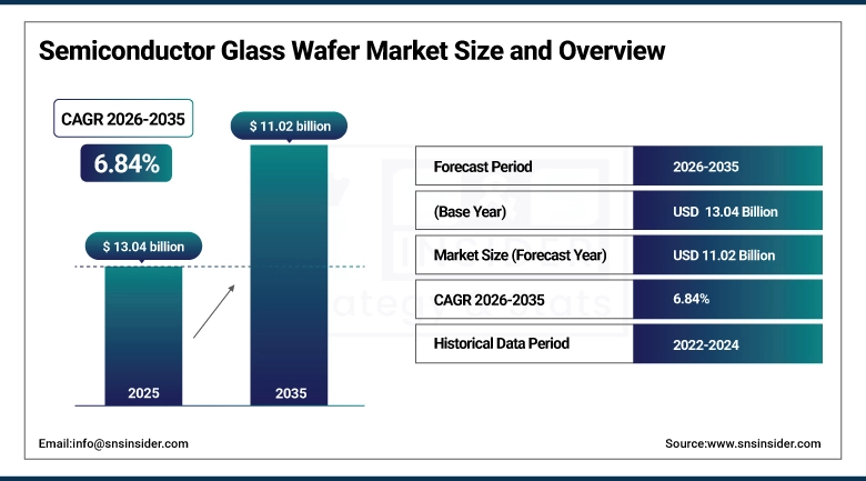
The Semiconductor Glass Wafer Market size was valued at USD 13.04 Billion in 2025 and is projected to reach USD 11.02 Billion by 2035, growing at a CAGR of 6.84% during 2026–2035.
The Semiconductor Glass Wafer market is all set to grow at the rate of a breed over the years with advancements in advanced packaging as the growing need for high-performance large-format glass substrates become pivotal in electronics. This also enables high density multi-chip assemblies and next-generation AI, HPC and high-speed computing applications, all of which require better electrical performance, better flatness and better thermal stability over traditional silicon-based materials which glass wafers provide. Because of their capability of supporting higher integration and material saving over conventional silicon wafer technology, they are a key material for scalable, high-efficiency semiconductor manufacturing. Ongoing USPs related to the glass wafer scale, surface treatment, and precision engineering, are widening the global market prospect in the coming future.
In Dec 2025, Rapidus unveils a 600x600 mm glass panel prototype tailored for high-performance AI packages; plans mass production by 2028 to rival TSMC's advanced packaging factors.
Semiconductor Glass Wafer Market Size and Forecast:
-
Market Size in 2025: USD 13.04 Billion
-
Market Size by 2035: USD 11.02 Billion
-
CAGR: 6.84% during 2026–2035
-
Base Year: 2025
-
Forecast Period: 2026–2035
-
Historical Data: 2022–2024
To Get more information on Semiconductor Glass Wafer Market - Request Free Sample Report
Semiconductor Glass Wafer Market Highlights:
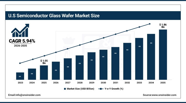
The U.S. Semiconductor Glass Wafer Market size was valued at USD 1.05 Billion in 2025 and is projected to reach USD 1.86 Billion by 2035, growing at a CAGR of 5.94% during 2026–2035, on the back of increasing demand for advanced semiconductors, MEMS devices & photonics needs in consumer electronics, automotive, aerospace, and industrial sectors, supported by vigorous R&D investments in the materials & capabilities, increase in the variances of photonic devices, wide-ranging technological innovations especially in the domain of semiconductor manufacturing process as well as government infrastructural schemes promoting domestic semiconductor industry as well as advanced wafer manufacturing market.
Semiconductor Glass Wafer Market Drivers:
-
Growth Opportunities in High-Performance Semiconductor Glass Wafers with Advanced Surface Treatments
Increasing demand for semiconductor glass wafers for greater optical clarity, lower reflections and improved surface qualities from consumer electronics and automotive displays is accelerating growth. Surface treatments including anti-reflective coatings and matte finishes not only assist in readability and image sharpness and color accuracy but do so in both miniaturized and high-resolution applications. Specialty glass wafer manufacturers can take advantage of this trend by supplying precision-engineered materials designed for use in AI, HPC and next-generation electronics. Increasing emphasis on display performances with the advent of chemical and optical treatments a sample of the growing semiconductor glass wafer market.
In Dec 2025, Corning’s Gorilla™ Matte Pro and SurfaceIQ™ received CES 2026 Innovation Awards for enhancing display readability and reducing glare in consumer electronics and automotive applications.
Semiconductor Glass Wafer Market Restraints:
-
Navigating Production and Innovation Challenges in the Semiconductor Glass Wafer Market
The semiconductor glass wafer market has many challenges which might affect the growth of the market. The high cost of production, including precision manufacturing and surface treatment, creates impediments for smaller suppliers. This calls for advance R&D and process control to meet its stringent thermal, chemical & mechanical specifications with strict quality and flatness requirement. Production can also be delayed or more expensive because supply chain disruptions, particularly with raw materials and specialty glass compositions. Finally, emerging semiconductor technologies like AI and HPC chips are characterized by rapid development cycles which impose further sustainability challenges for the manufacturers that need to scale the technology while meeting yield, reliability, and sustainability specifications.
Semiconductor Glass Wafer Market Opportunities:
-
Growth Potential in Precision Glass for Advanced Semiconductor Packaging
Demand for precision glass wafers and panels is growing strongly as the applications of AI and high-performance computing (HPC) chips become more complex and minituarised. Thinner materials with tighter thickness variation, better mechanical, thermal, and chemical properties, and improved surface quality, provide for higher yields, 3D IC integration, and fan-out wafer-level or panel-level packaging. Specialty glass suppliers that have developed specialty glass optimized for advanced semiconductor applications are best positioned to benefit from growth opportunities across AI, HPC, and other high-end performance electronics markets, facilitating innovation and scaling of chips.
In Sept 2025, SCHOTT highlights thinner and homogenous precision glass wafers and panels with advanced material features for AI/HPC chip packaging.
Semiconductor Glass Wafer Market Segment Highlights:
-
By Type: Dominant – Borosilicate Glass (48.20% → 41.80%); Fastest-Growing – Fused Silica (22.70% → 32.30%, CAGR 10.60%)
-
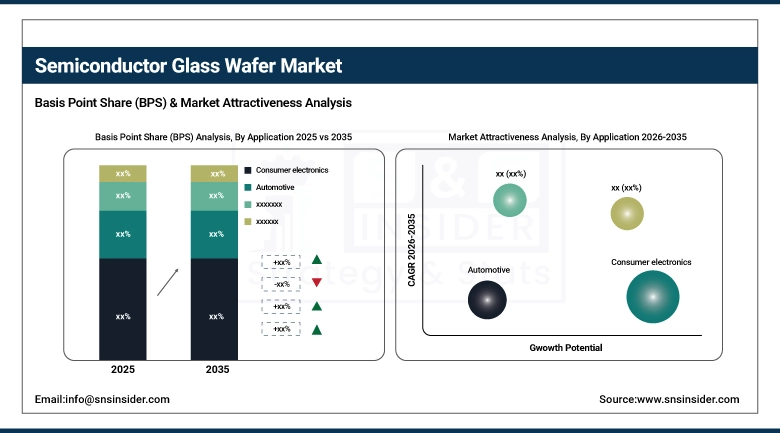
By Application: Dominant – Consumer Electronics (34.50% → 30.50%); Fastest-Growing – Automotive (25.30% → 27.70%, CAGR 7.81%)
-
By Technology: Dominant – Polished Glass Wafers (39.50% → 35.50%); Fastest-Growing – Bonded Glass Wafers (20.20% → 21.80%, CAGR 7.66%)
-
By Product Type: Dominant – 200 mm to 300 mm (35.00% → 35.00%); Fastest-Growing – Above 300 mm (26.80% → 33.20%, CAGR 9.13%)
Semiconductor Glass Wafer Market Segment Analysis:
Consumer Electronics Dominance and Rapid Growth in Automotive
Consumer electronics is the largest segment of the semiconductor glass wafer market, driven by the increasing usage of smartphones, laptops, tablets, and other smart devices. The automotive segment is the fastest-growing segment of the semiconductor glass wafer market. The increasing adoption of intelligent vehicle technologies, electric vehicles, and autonomous vehicles is driving the growth of the semiconductor glass wafer market in the automotive sector.
Borosilicate Glass Dominance and Rapid Growth in Fused Silica
The Semiconductor Glass Wafer Market covered under the semiconductor glass wafer has been segmented across three types of glass which are borosilicate, quartz and others where type borosilicate represented the largest segment owing to its excellent thermal stability, chemical resistance and overall wide usage in different end use industry especially in consumer electronics, industrial and photonics applications. fused silica is the fastest adopted and growing segment, due to increasing application in various high-end electronics and industrial technologies including high-purity & low-expansion substrate for advanced semiconductor manufacturing MEMS & photonics applications.
Polished Glass Wafer Dominance and Rapid Growth in Bonded Glass Wafers
Polished glass wafers remain the dominant segment of the semiconductor glass wafer market. This is because polished glass wafers offer the highest surface flatness and precision, which is critical in the semiconductor, MEMS, and photonics industries. The bonded glass wafer type segment is the fastest-growing segment of the semiconductor glass wafer market. This is driven by the increasing need for multi-layer packaging, heterogeneous integration, and advanced semiconductor technologies. This is helping the semiconductor glass wafer market to witness significant growth in the automotive, industrial, and consumer electronics segments..
200 mm to 300 mm Dominance and Rapid Growth in Above 300 mm Wafers
The 200 mm to 300 mm semiconductor glass wafer segment is the dominant segment of the semiconductor glass wafer market. This is driven by the established usage of semiconductor and MEMS devices. The above 300 mm semiconductor glass wafer segment is the fastest-growing segment of the semiconductor glass wafer market. This is driven by the need for large substrates in the field of high-performance computing, advanced packaging, and next-generation semiconductor technologies.
Semiconductor Glass Wafer Market Regional Highlights:
-
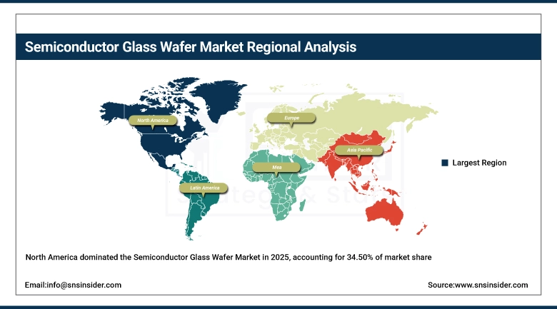
North America: 34.50% (2025) → 30.50% (2035), Dominant Region with strong aerospace, defense, and advanced electronics demand, maintaining the largest market share despite gradual decline (CAGR 5.53%)
-
Asia-Pacific: 30.50% (2025) → 36.30% (2035), Fastest-Growing Region driven by rapid semiconductor, MEMS, and photonics adoption (CAGR 8.70%)
-
Europe: 24.70% (2025) → 22.30% (2035), Steady Growth Region supported by automotive, industrial, and semiconductor R&D investments (CAGR 5.75%)
-
South America: 5.10% (2025) → 5.90% (2035), Moderate Growth Region with gradual expansion due to increasing electronics and industrial adoption (CAGR 8.40%)
-
Middle East & Africa: 5.20% (2025) → 5.00% (2035), Emerging Growth Region supported by infrastructure, MEMS, and photonics demand (CAGR 6.42%)
Semiconductor Glass Wafer Market Regional Analysis:
North America Semiconductor Glass Wafer Market Insights:
The North America Semiconductor Glass Wafer Market is seeing growth due to rising demand for well-performing semiconductors, MEMS devices, and advanced packaging. These factors attribute to the given US and Canada market being highly competitive, with few players dominating the domestic market, supported by constant technological innovations and heavy investments in R&D made by players in these countries. Also, increasing utilization in industries like aerospace, automotive, electronics, & supporting government initiatives promoting semiconductor production help North America to be a dominant region in the global glass wafer market.
Get Customized Report as per Your Business Requirement - Enquiry Now
U.S. Semiconductor Glass Wafer Market Insights:
The continuous increase in demand for advanced semiconductors, MEMS and photonics, coupled with increasing focus on R&D and Technological innovations, growth of government-backed programs and initiatives to promote business area are some of the driving factors of the United States Semiconductor Glass Wafer Market.
Asia-Pacific Semiconductor Glass Wafer Market Insights:
The Asia Pacific is the most dominating region in the world semiconductor glass wafers market due to strong demand from countries such as China, Japan, South Korea, and Taiwan. Market growth boosted as semiconductor manufacturing, advanced packaging, MEMS, and photonics applications accelerate. The increased presence of key players in local production and R&D facilities along with government support coupled with technological advances will continue to strengthen the dominance of this region over the semiconductor glass wafer industry, thus making the Asia-Pacific the largest and fastest growing market during the forecast period.
China Semiconductor Glass Wafer Market Insights:
China continues to account the greatest commitment to the Semiconductor Glass Wafer market, influenced via the big semiconductor fabricating base, sturdy R&D investments, results of nearby authorities guidelines, and boosting demand for new packaging, MEMS, and photonics applications.
Europe Semiconductor Glass Wafer Market Insights:
he Europe Semiconductor Glass Wafer market is growing moderately, supported by steady demand from the automotive, electronics, and industrial sectors. Key players in Germany, France, and the UK are investing in advanced glass wafer technologies, enhancing production efficiency and quality. Government initiatives promoting semiconductor innovation and research, coupled with increasing adoption of MEMS, photonics, and advanced packaging applications, are contributing to sustainable market growth, positioning Europe as a significant yet gradually expanding player globally.
Germany Semiconductor Glass Wafer Market Insights:
The growth of Germany Semiconductor Glass Wafers market is expected to develop at a moderate pace, due to high automotive and industrial demand, constant R&D investments, rapid technological advancements, the implementations of advanced packaging and MEMS technologies, and advantageous governmental policies.
Latin America Semiconductor Glass Wafer Market Insights:
The Latin America Semiconductor Glass Wafer market is witnessing steady growth, driven by increasing adoption of semiconductor technologies across automotive, electronics, and industrial applications. Rising investments in local manufacturing facilities and technological advancements are enhancing production capabilities. Increasing investments in domestic production facilities and technology are improving manufacturing capabilities. Government-driven plans to incentivize innovation and semiconductor research are paying off in major markets like Brazil and Mexico. The demand for MEMS, photonics, and advanced packaging solutions in the region underpins gradual market expansion.
Brazil Semiconductor Glass Wafer Market Insights:
Brazil leads the Latin America Semiconductor Glass Wafer market, driven by strong semiconductor manufacturing, growing demand for MEMS and photonics applications, and supportive government initiatives promoting technology development and local production.
Middle East & Africa (MEA) Semiconductor Glass Wafer Market Insights:
The Middle East & Africa Semiconductor Glass Wafer market is growing gradually, supported by increasing adoption of semiconductor technologies in electronics, automotive, and industrial sectors. Investments in local manufacturing, technological advancements, and government initiatives to boost innovation are driving market development. Gradual growth is also fueled by rising demand for MEMS, photonics, and advanced packaging applications across the region.
United Arab Emirates Semiconductor Glass Wafer Market Insights:
The United Arab Emirates (UAE) is currently the dominant country, driven by its growing electronics manufacturing sector, investments in semiconductor infrastructure, and government initiatives supporting advanced technology adoption. Saudi Arabia is also emerging as a key player, but the UAE leads in production and market presence.
Semiconductor Glass Wafer Market Competitive Landscape:
GlobalFoundries – Created in 2009, GlobalFoundries is a leading semiconductor foundry that supplies best-in-class high-performance, power-efficient automotive, mobile, IoT and communications chips. GF has a global manufacturing footprint in the U.S., Europe and Asia with a focus on silicon photonics, advanced process technologies, and flexible, reliable and scalable semiconductor solutions fоr customers around the globe.
-
In Sept 2025, GlobalFoundries and Corning launched GlassBridge detachable fiber connectors, enabling co-packaged optics for high-bandwidth, power-efficient AI datacenter connectivity.
AGC Inc. Founded in 1907, AGC Inc.is the largest glass, chemicals and advanced materials player in the world. Together with advanced high-precision glass substrates, optical components and semiconductor materials, the company is driving sustainable, recycling, and innovative solutions for electronics, automotive and industrial applications, supporting advanced semiconductor manufacturing across the globe.
-
In Aug 2025, AGC exhibited glass carriers, Through Glass Vias, CMP slurries, and polymer optical waveguides, emphasizing sustainable fluorinated material recycling.
Semiconductor Glass Wafer Market Key Players:
-
AGC Inc.
-
Corning Incorporated
-
SCHOTT AG
-
Plan Optik AG
-
Shin‑Etsu Chemical Co. Ltd.
-
Sumco Corporation
-
Siltronic AG
-
MEMC / SunEdison Semiconductor
-
SAS (Sino‑American Silicon Products)
-
Okmetic Oy
-
Shenhe FTS
-
SST (Shanghai Sinyu Technology)
-
JRH (Jingrui High‑Tech)
-
LG Siltron
-
Bullen Ultrasonics
-
Coresix Precision Glass Inc.
-
Hoya Candeo Optronics Corp.
-
Mosaic Microsystems
-
Nano Quarz Wafer
-
Specialty Glass Products
| Report Attributes | Details |
|---|---|
| Market Size in 2025 | USD 13.04 Billion |
| Market Size by 2035 | USD 25.27 Billion |
| CAGR | CAGR of 6.84% From 2026 to 2035 |
| Base Year | 2025 |
| Forecast Period | 2026-2035 |
| Historical Data | 2022-2024 |
| Report Scope & Coverage | Market Size, Segments Analysis, Competitive Landscape, Regional Analysis, DROC & SWOT Analysis, Forecast Outlook |
| Key Segments | • By Type(CPLD (Complex Programmable Logic Device) and FPGA (Field Programmable Gate Array)) • By Application(Consumer Electronics, Automotive & Transportation, Industrial Automation, Telecommunications and Aerospace & Defense) • By Product Type(OEMs (Original Equipment Manufacturers), System Integrators and Research & Academic Institutions) • By Technology/Feature(Reprogrammable PLDs, Non-Reprogrammable PLDs, Low-Power PLDs and High-Performance PLDs) |
| Regional Analysis/Coverage | North America (US, Canada), Europe (Germany, UK, France, Italy, Spain, Russia, Poland, Rest of Europe), Asia Pacific (China, India, Japan, South Korea, Australia, ASEAN Countries, Rest of Asia Pacific), Middle East & Africa (UAE, Saudi Arabia, Qatar, South Africa, Rest of Middle East & Africa), Latin America (Brazil, Argentina, Mexico, Colombia, Rest of Latin America). |
| Company Profiles | AGC Inc., Corning Incorporated, SCHOTT AG, Plan Optik AG, Shin‑Etsu Chemical Co. Ltd., Sumco Corporation, Siltronic AG, MEMC / SunEdison Semiconductor, SAS (Sino‑American Silicon Products), Okmetic Oy, Shenhe FTS, SST (Shanghai Sinyu Technology), JRH (Jingrui High‑Tech), LG Siltron, Bullen Ultrasonics, Coresix Precision Glass Inc., Hoya Candeo Optronics Corp., Mosaic Microsystems, Nano Quarz Wafer, Specialty Glass Products |
Get in Touch
