Semiconductor Plasma Dicing Tape Market Size Analysis:
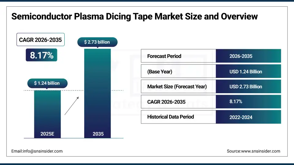
The Semiconductor Plasma Dicing Tape Market size was valued at USD 1.24 Billion in 2025 and is projected to reach USD 2.73 Billion by 2035, growing at a CAGR of 8.17% during 2026-2035.
The Semiconductor Plasma Dicing Tape Market is growing as a result of the rising demand for high-precision wafer dicing in the semiconductor industry. The increasing adoption of 3D ICs, MEMS, and LED devices is driving the demand for efficient dicing solutions. The use of the tape helps to reduce wafer damage and increase yield.
Over 65% of 3D IC and chiplet-based packages produced in 2024 require plasma dicing processes, which rely on specialized dicing tapes that maintain wafer integrity during deep etching. TSMC, Intel, and Samsung now use plasma dicing in over 40% of their advanced node.
Market Size and Growth Projection:
-
Market Size in 2025 USD 1.24 Billion
-
Market Size by 2035 USD 2.73 Billion
-
CAGR of 8.17% From 2026 to 2035
-
Base Year 2025
-
Forecast Period 2026-2035
-
Historical Data 2022-2024
To Get More Information On Semiconductor Plasma Dicing Tape Market - Request Free Sample Report
Semiconductor Plasma Dicing Tape Market Trends
-
Rising Demand for Advanced Semiconductor Devices such as growth in MEMS, LEDs, and 3D IC production is driving adoption of plasma dicing tapes.
-
Increased Adoption of UV-Curable and High-Adhesion Tapes and these tapes improve wafer yield and reduce damage, enhancing manufacturing efficiency.
-
Expansion of Semiconductor Fabrication and Packaging Facilities due to Growing production capabilities are fueling demand for advanced dicing solutions.
-
Integration with Automation enhances efficiency, scalability, and process reliability in semiconductor manufacturing.
-
Development of eco-friendly tapes, collaborations between manufacturers, and rising semiconductor demand create significant growth opportunities.
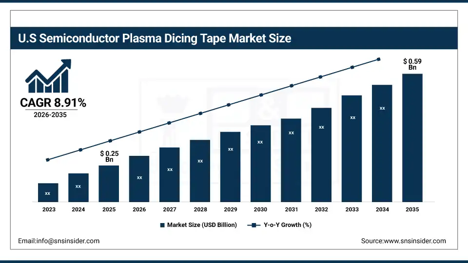
U.S. Semiconductor Plasma Dicing Tape Market Size Outlook
The U.S. Semiconductor Plasma Dicing Tape Market was valued at USD 0.25 Billion in 2025 and is projected to reach USD 0.59 Billion by 2035, growing at a CAGR of 8.91% from 2026 to 2035. The Semiconductor Plasma Dicing Tape Market is growing due to the rising demand for high-performance and miniaturized semiconductor devices. The rising production of MEMS, LEDs, and advanced ICs is leading to the demand for accurate wafer dicing solutions. The market is experiencing the use of UV-curable and high-adhesion tapes.
Semiconductor Plasma Dicing Tape Market Growth Drivers:
-
Rising Demand for High-Precision Wafer Dicing in Advanced Semiconductor Manufacturing Driving Market Growth.
The market is driven by the increasing production of MEMS, LEDs, and 3D ICs, which demand advanced dicing, and the adoption of UV-curable and high-adhesion tapes, which enhance the yield and resistance of wafers. The growth of semiconductor fabrication and packaging lines is driving the demand, and the evolution of more efficient tape materials is also propelling the market.
UV-Curable Tapes: The use of UV-release dicing tapes has grown to over 60% of advanced packaging lines in 2025, allowing for residue-free and clean debonding after plasma dicing. The tapes also lower post-dicing defects by as much as 40% compared to thermal-release tapes.
Semiconductor Plasma Dicing Tape Market Restraints:
-
High Cost and Specialized Handling Requirements Limiting Adoption of Semiconductor Plasma Dicing Tape
The price of the advanced plasma dicing tapes is high, which increases the manufacturing cost of semiconductors, and the handling and storage process is complex. The incompatibility of the product with some wafers may limit its use, and it also requires expert labor to apply and remove the tape. All these factors may work together to slow down the adoption rate, particularly in small semiconductor manufacturing facilities.
Semiconductor Plasma Dicing Tape Market Opportunities:
-
Technological Advancements in Tape Materials and 3D IC Applications Expanding Semiconductor Plasma Dicing Market
The emergence of UV-curable, high-adhesive, and eco-friendly tapes with better performance is a positive trend, and their use in 3D ICs, MEMS, and LEDs is growing rapidly. The integration of tapes with automated dicing systems is increasing efficiency, and partnerships between tape suppliers and semiconductor firms are fueling innovation. The plasma dicing tape market has immense growth opportunities due to the rise of new markets and the demand for semiconductors.
In 2025, over 65% of advanced semiconductor packaging lines (especially at TSMC, Samsung, and Intel) use UV-curable dicing tapes due to their clean, rapid debonding capability. These tapes reduce post-processing cleaning steps by up to 50%, improving throughput.
Semiconductor Plasma Dicing Tape Market Segment Analysis
-
By Product Type, UV Release Dicing Tape led the market with approximately 42.62% share in 2024, while Non-UV Dicing Tape was the fastest-growing segment with a CAGR of 8.75%.
-
By Application, Wafer Dicing dominated the market with around 45.23% share in 2024, whereas Die Attachment recorded the fastest growth with a CAGR of 8.79%.
-
By Material, Polyolefin led the market with approximately 51.43% share in 2024, while Polyvinyl Chloride emerged as the fastest-growing material with a CAGR of 8.80%.
-
By End-User, Semiconductor Manufacturers held the largest share at about 56.21% in 2024, while Electronics Manufacturers were the fastest-growing end-user segment with a CAGR of 8.78%.
By End-User, Semiconductor Manufacturers Lead While Electronics Manufacturers Grow Fastest
The semiconductor manufacturers are the leaders in the plasma dicing tape market, as they are the key users of the plasma dicing tape in the wafer dicing and high-precision packaging processes. The need for improved yields and efficient processing techniques among semiconductor manufacturers triggers the demand for advanced plasma dicing tapes. On the other hand, the electronics manufacturers are expanding at the fastest rate due to the rising usage of plasma dicing tapes in MEMS, LEDs, and new semiconductor devices.
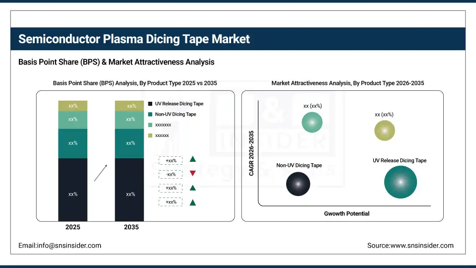
By Product Type, UV Release Dicing Tape Leads Market While Non-UV Dicing Tape Registers Fastest Growth
UV Release Dicing Tape currently dominates the semiconductor plasma dicing tape market with the largest market share, thanks to its accuracy and consistency in wafer dicing. On the other hand, Non-UV Dicing Tape is currently growing at the fastest rate due to its economical nature and adaptability to different types of wafers. Its adoption in new semiconductor technology also fuels its demand. This shows the dynamic nature of the market in terms of segmentation offered by the product type.
By Application, Wafer Dicing Dominate While Die Attachment Shows Rapid Growth
The market for semiconductor plasma dicing tapes is dominated by the wafer dicing segment, as this is still the most prominent method used for separating chips from semiconductor wafers. The demand for advanced packaging and assembly techniques is driving the die attachment segment at a fast pace. The adoption of these tapes in new technologies such as MEMS and LEDs is also propelling the market for semiconductor plasma dicing tapes.
By Material, Polyolefin Lead While Polyvinyl Chloride Registers Fastest Growth
Polyolefin currently holds the largest market share in the semiconductor plasma dicing tape market because of its strong adhesive properties, heat resistance, and compatibility with different types of semiconductors. On the other hand, polyvinyl chloride (PVC) is growing at the fastest rate due to its economical nature and adaptability with different processing methods. The rising adoption in the latest semiconductor technology is also fueling the demand for PVC.
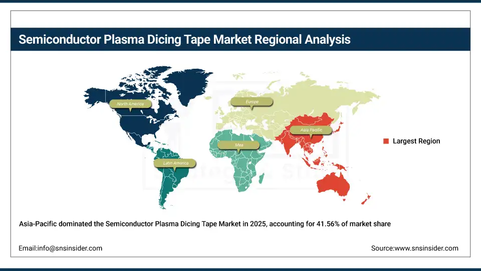
Asia-pacific Semiconductor Plasma Dicing Tape Market Insights
In 2025 Asia-Pacific dominated the Semiconductor Plasma Dicing Tape Market and accounted for 41.56% of revenue share, this leadership is due to the rising semiconductor manufacturing activities, increasing production of MEMS, LEDs, and 3D ICs, and expanding wafer fabrication facilities. High demand for advanced packaging technologies and cost-effective dicing solutions is driving adoption. Technological advancements in tape materials and precision dicing are supporting market growth. Government initiatives and investments in smart manufacturing further boost the region’s market.
Get Customized Report as Per Your Business Requirement - Enquiry Now
China Semiconductor Plasma Dicing Tape Market Insights
China’s market is expanding due to its dominant semiconductor fabrication industry, increasing production of advanced ICs, MEMS, and LED devices, and strong government support for semiconductor technology. Adoption of high-precision plasma dicing tapes improves yield and reduces wafer damage.
North America Semiconductor Plasma Dicing Tape Market Insights
North America is expected to witness the fastest growth in the Semiconductor Plasma Dicing Tape Market over 2026-2035, with a projected CAGR of 9.01% due to its established semiconductor industry, high adoption of MEMS, LEDs, and 3D ICs, and advanced wafer fabrication facilities. Demand for UV-curable and high-adhesion tapes to improve yield and reduce wafer damage is increasing.
U.S. Semiconductor Plasma Dicing Tape Market Insights
The U.S. market is expanding due to the increasing production of MEMS, LEDs, and 3D ICs, which require high precision in wafer dicing. The use of UV-curable and high-adhesion tapes is increasing, which improves efficiency and yield. The growth of semiconductor fabrication and packaging facilities is driving demand.
Europe Semiconductor Plasma Dicing Tape Market Insights
The European market is a promising one due to the increasing demand for semiconductor packaging, MEMS, LEDs, and 3D ICs. The use of high-precision plasma dicing tapes is increasing, which improves the yield of wafers. Technological advancements in UV-curable and high-adhesion tapes are increasing efficiency.
Germany Semiconductor Plasma Dicing Tape Market Insights
Germany’s market is growing due to its strong semiconductor and electronics manufacturing industry, increasing adoption of MEMS and LED devices, and focus on high-quality wafer dicing solutions. Advanced plasma dicing tapes improve production yield and minimize wafer damage.
Latin America (LATAM) and Middle East & Africa (MEA) Semiconductor Plasma Dicing Tape Market Insights
The market in LATAM and MEA is experiencing moderate growth due to rising semiconductor and electronics manufacturing activities. The growing use of UV-curable and high-adhesion tapes in wafer dicing enhances efficiency. Smart manufacturing and technology development are also encouraging market growth. The limited but increasing emphasis on advanced packaging technology is driving demand.
Semiconductor Plasma Dicing Tape Market Competitive Landscape:
Nitto Denko Corporation is a world leader in functional materials and a key player in the semiconductor plasma dicing tape market with its high-performance and plasma-resistant adhesive tapes. The company’s products are in high demand in 3D ICs, MEMS, and advanced packaging, where reliability, low outgassing, and clean debonding are essential.
-
In May 2024, Nitto Denko launched its NF735 series plasma dicing tape, designed for 2.5D/3D packaging and HBM applications, featuring halogen-free composition and superior adhesion stability under deep plasma etching. The tape is now in volume production use at Samsung’s Pyeongtaek facility and selected TSMC backend lines.
Furukawa Electric Co. Ltd. is a major player in the semiconductor materials industry, recognized for its precision-engineered dicing and bonding tapes specifically designed for the challenging plasma dicing process. The company is committed to the development of tapes with low thermal expansion, high UV transmittance, and superior wafer retention properties, which are essential in 3D-stacked devices and MEMS processing.
-
In April 2024, Furukawa Electric introduced the F-DICE™ 8000P tape, optimized for ultra-thin (≤25μm) silicon wafers used in fan-out packaging, offering 30% lower warpage and improved debonding consistency. The product is being evaluated by ASE and Amkor for integration into next-gen AI chip packaging lines.
Mitsui Chemicals, Inc. is a leader in the development of next-generation dicing tapes with a strong emphasis on sustainability, functionality, and compatibility with automated semiconductor manufacturing. The company provides a variety of UV-release and temporary bonding tapes designed for plasma dicing, especially in 3D NAND, CMOS image sensors, and power devices.
-
In March 2024, Mitsui Chemicals launched TAPEXIA™ Z-77, a bio-based temporary bonding tape with low outgassing and high thermal resistance, targeting environmentally conscious fabs in Europe and Japan.
LINTEC Corporation is a leading innovator in precision adhesive materials, and its Wafer Support Systems (WSS) business is a leader in plasma dicing tape. LINTEC’s tapes are broadly used for their high adhesion control, clean release, and suitability for thin-wafer and TSV processing in 3D ICs and MEMS. The company is also working to improve its product lineup with smart materials, such as tapes with real-time stress monitoring and AI-optimized performance.
-
In June 2024, LINTEC unveiled AutoAdhere™-X, an AI-integrated dicing tape system that dynamically adjusts adhesion based on real-time wafer stress feedback, reducing breakage by up to 40%. The solution is now deployed in TSMC’s CoWoS packaging lines and selected Intel IDM 2.0 facilities.
Semiconductor Plasma Dicing Tape Companies are:
-
Furukawa Electric Co., Ltd.
-
Mitsui Chemicals, Inc.
-
LINTEC Corporation
-
Sumitomo Bakelite Co., Ltd.
-
AI Technology, Inc.
-
Pantech Tape Co., Ltd.
-
Mitsubishi Chemical Corporation
-
Ultron Systems, Inc.
-
3M Company
-
Daest Coating India Pvt. Ltd.
-
Adwill (Hitachi Chemical Co., Ltd.)
-
Teraoka Seisakusho Co., Ltd.
-
Loadpoint Limited
-
QES Group Berhad
-
Sekisui Chemical Co., Ltd.
-
Teraoka Seisakusho Co., Ltd.
-
Shanghai Xinke Semiconductor Material Co., Ltd.
-
PULS Electronic AG
| Report Attributes | Details |
|---|---|
| Market Size in 2025 | USD 1.24 Billion |
| Market Size by 2035 | USD 2.73 Billion |
| CAGR | CAGR of 8.17% From 2026 to 2035 |
| Base Year | 2025 |
| Forecast Period | 2026-2035 |
| Historical Data | 2022-2024 |
| Report Scope & Coverage | Market Size, Segments Analysis, Competitive Landscape, Regional Analysis, DROC & SWOT Analysis, Forecast Outlook |
| Key Segments | • By Product Type (UV Release Dicing Tape, Non-UV Dicing Tape, Thermal Release Dicing Tape, and Others) • By Application (Wafer Dicing, Die Attachment, Packaging, and Others) • By Material (Polyolefin, Polyvinyl Chloride, Polyethylene Terephthalate, and Others) • By End-User (Semiconductor Manufacturers, Electronics Manufacturers, and Others) |
| Regional Analysis/Coverage | North America (US, Canada), Europe (Germany, UK, France, Italy, Spain, Russia, Poland, Rest of Europe), Asia Pacific (China, India, Japan, South Korea, Australia, ASEAN Countries, Rest of Asia Pacific), Middle East & Africa (UAE, Saudi Arabia, Qatar, South Africa, Rest of Middle East & Africa), Latin America (Brazil, Argentina, Mexico, Colombia, Rest of Latin America). |
| Company Profiles | Nitto Denko Corporation, Furukawa Electric Co., Ltd., Mitsui Chemicals, Inc., LINTEC Corporation, Denka Company Limited, Sumitomo Bakelite Co., Ltd., AI Technology, Inc., Pantech Tape Co., Ltd., Mitsubishi Chemical Corporation, Ultron Systems, Inc., 3M Company, Daest Coating India Pvt. Ltd., Adwill (Hitachi Chemical Co., Ltd.), Teraoka Seisakusho Co., Ltd., Loadpoint Limited, QES Group Berhad, Sekisui Chemical Co., Ltd., Teraoka Seisakusho Co., Ltd., Shanghai Xinke Semiconductor Material Co., Ltd., PULS Electronic AG. |
Frequently Asked Questions
Asia-Pacific dominated the Semiconductor Plasma Dicing Tape Market in 2025.
The UV Release Dicing Tape segment dominated during the projected period.
Growth is driven by rising demand for high-precision wafer dicing, growth in MEMS, LEDs, and 3D IC production, and adoption of advanced, high-adhesion, and UV-curable tapes.
The market was valued at USD 1.24 Billion in 2025 and is projected to reach USD 2.73 Billion by 2035.
The Semiconductor Plasma Dicing Tape Market is expected to grow at a CAGR of 8.17% during 2026–2035.
Get in Touch
