Thin Wafer Market Size:
Get More Information on Thin Wafer market - Request Sample Report
Thin Wafer Market Overview
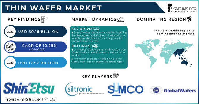
The Thin Wafer Market size was valued at USD 12.57 Billion in 2023 & expects good growth by reaching USD 30.16 billion till the end of 2032 at a CAGR of about 10.29 % during the forecast period 2024-2032.
The abundance of data is fueling an increase in the need for semiconductors. Efficient packaging is necessary for these essential chips in our electronics, as miniaturization trends continue. Thin wafers are the solution, and there is a promising outlook for substantial growth in the market for these extremely thin components. The growth of MEMS technology, combining electrical and mechanical parts in small devices for various applications, is also contributing to this. Highlighting this expansion, Infineon, a major semiconductor company, recently opened a huge €1.6 billion chip plant in Austria specifically tailored for manufacturing power electronics on 300-millimeter thin wafers. This investment highlights the increasing significance of thin wafers in addressing the needs of our data-centric society.
The conventional solar cell market is currently in control, but there is a promising opportunity in flexible, lightweight thin silicon solar cells. Yet, the potential of this exciting market has been hindered by the fragility of these extremely thin wafers, resulting in breakage while being manufactured. Scientists have created a novel technique called TSRR (thin silicon with reinforced ring) to enhance the durability of the wafers' edges. This method has effectively created thin silicon wafers that stand on their own and reached high efficiency (greater than 20%) in operating solar cells – all while maintaining a nearly zero rate of breakage. Even simulations indicate that improving the width of the ring in the TSRR design can increase effectiveness. The method has been verified to work well with current manufacturing processes, allowing for large-scale production to begin. Essentially, TSRR provides a remedy for the issue of fragility, which could open up the extensive market opportunities for thin silicon solar cells that are lightweight and flexible. This advancement may result in fresh uses for solar technology, marking a major breakthrough in the industry.
Market Dynamics
Drivers
-
Ever-growing digital consumption is driving the thin wafer market due to their ability to miniaturize electronics for more powerful and portable devices.
The growing amount of data we generate drives an endless need for increasingly powerful semiconductor devices. The small brains found in electronic devices, such as microprocessors and memory chips, play a crucial role in our digital society, enabling the functioning of devices like smartphones, laptops, and data centers housing vast amounts of data. Picture a data center - a large storage facility packed with rows of computer racks. Each rack houses multiple servers, all requiring strong processors and memory to manage the continuous data flow. With the exponential growth of data, data centers constantly need increased processing power. This results in a growing need for these small semiconductor devices. This is the point where thin wafers play a role. These are the extremely slim units utilized in creating these necessary parts. Similar to how constructing a skyscraper necessitates durable, lightweight materials, slim wafers provide an answer for fitting increased processing capability into tighter areas.
-
The miniaturization needs of MEMS technology in portable health monitors and other tiny devices are driving the thin wafer market.
MEMS technology is leading the way in the shrinking world of technology. Picture a small device that is small enough to be placed on the tip of your finger, but has the capability to detect your movements, gauge pressure, or identify chemicals. These are Microelectromechincal Systems (MEMS), examples of engineering excellence that combine electrical and mechanical parts at a very small size. Thin wafers, extremely thin slices of silicon or other materials, offer the perfect foundation for constructing these tiny wonders. Their accurate measurements and polished exteriors enable the creation of detailed electrical circuits and fragile mechanical structures through micro fabrication methods on their surface. This enables the development of small beams, gears, and chambers that collaborate to carry out intricate tasks. A thin wafer with a MEMS accelerometer could be crucial in tracking your movements and activity levels. In the same way, a thin-wafer-based MEMS pressure sensor installed in your car's airbag system has the ability to detect a sudden impact and initiate deployment within milliseconds. The uses are wide-ranging and constantly growing, ranging from the gyroscopes in your smartphone that maintain game orientation to the microfluidic channels in medical diagnostic chips. Thin wafers provide an ideal blend of durability, bendability, and ease of production for MEMS technology. They enable the development of tiny, dependable, and affordable devices that are changing different industries. When you use a modern electronic device, think about the hidden power of thin wafers that make MEMS technology possible and bring innovative features to our fingertips.
Restraints
-
Limited efficiency gains in thin wafers can hinder their competitiveness in the solar cell market.
The resource advantage of thin silicon wafers comes at a cost: lower efficiency. Imagine a solar cell as a light sponge. Thicker wafers, like denser sponges, soak up more sunlight, generating more power. Thinner versions capture less light, sacrificing efficiency. The challenge lies in finding the sweet spot – a wafer thin enough to save material but thick enough to absorb light effectively. Researchers are exploring light-trapping designs and light-concentrating materials to boost light absorption in thin wafers, paving the way for a more sustainable and efficient solar cell technology.
-
The major obstacle of beginning in thin wafers can lead to expensive challenges.
Entering the world of thin wafers offers great potential, but for newcomers, the challenge can be likened to scaling a mountain. Picture a large factory space - to produce these thin wafers, you must have a range of advanced machinery. Advanced equipment for precision thinning of silicon wafers, as well as cutting-edge cleaning and processing tools, all have a high cost. This financial hardship poses a significant obstacle, especially for newcomers and smaller businesses. The elevated expenses can suppress rivalry and impede creativity within the marketplace. Picture a skilled businessperson with a fantastic concept for an innovative thin-wafer gadget. Yet, their aspirations may be thwarted by the substantial amount of funds required to begin, restricting the variety of ideas and strategies present in the market. Sustaining these sophisticated machines also necessitates continuous financial commitment. Routine maintenance, adjustment, and possible enhancements contribute to the overall expenses.
Thin Wafer Market Segment Analysis
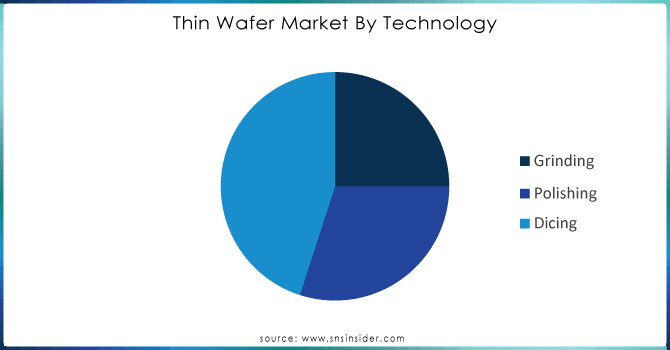
In the Thin Wafer Market, Dicing holds a 45% market share in 2023, led by technology. The need for ultra-thin wafer dicing arises from the increasing memory capacity and continuous package miniaturization. Lately, there has been an increase in the utilization of RFID tags and SIP (system in package) in smartphones and other compact electronic devices. Consequently, there has been a rapid rise in the manufacturing of semiconductor dies that are 100 µm thin or thinner. The growing demand for thin wafers has become an essential expertise for many integrated device manufacturers. The increasing requirement for wafer dicing machines that can operate at high speeds and are highly resistant to breakage has caused a rise in the demand for this type of equipment.
Need Customized Research Report on Thin Wafer Market - Enquiry Now
By Application, CMOS Image Sensor (CIS) dominates with a 25% market share in 2023. Small cameras called CMOS image sensors (CIS) are commonly seen in smartphones and various devices, driving the need for thin wafers. As our gadgets shrink, the chips they need also get smaller, leading to the need for standard and very thin wafers in their manufacturing. Thin wafers are perfect for creating these small CIS chips. The growing demand for top-notch cameras in increasingly compact devices is a major driver of the successful thin wafer market.
Thin Wafer Market Regional Analysis
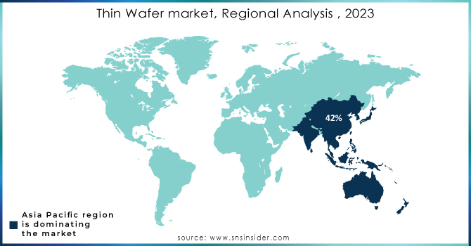
Asia Pacific dominates the thin wafer market in 2023 with a market share of 42%. Asia Pacific is crucial for the growth of the electrical and electronics sector. Several top thin wafer manufacturers, including Shin-Etsu Chemical Co., Ltd. (Japan), SUMCO Corporation (Japan), and Global Wafers Co., Ltd. Asia Pacific is where DISCO Corporation (Japan) and Taiwan are located. The rapid expansion of the Asia Pacific region is due to the increasing popularity of advanced consumer electronics like wearables and smart home gadgets in China and Japan. Due to favorable economic conditions and rising demand for consumer electronics, significant growth in the Asia Pacific region is anticipated in the global semiconductor market. Due to the affordable labor in Asia Pacific, a majority of thin wafers and wafer thinning equipment are produced in the region and then shipped to different areas.
North America region is the fastest growing in the thin wafer market, holding a significant 23% market share in 2023. The United States has a huge consumer electronics sector. The constant desire for smaller and more powerful electronics drives the demand for thin wafers. In addition to consumer electronics, healthcare and automotive industries in North America also have a significant impact. Consider the most recent medical imaging machinery or cutting-edge driver-assistance systems found in vehicles – these technologies frequently depend on slender wafer-based parts. North America's position is further solidified by the presence of top thin wafer manufacturers in the region. These established participants not just serve the needs of the local market but also stimulate creativity within the sector.
Key Players
Some of the major players are Shin-Etsu Chemical Co., Ltd. (Japan), SUMCO Corporation (Japan), GlobalWafers Co., Ltd. (Taiwan), Siltronic (Germany), SK Siltron (South Korea), SUSS MicroTec (Germany), Soitec (France), DISCO Corporation (Japan), 3M (US), Applied Materials (US), Mechatronic Systemtechnik (Austria), Synova (Switzerland), Brewer Science (US), EV Group (Austria), Wafer Works Corporation (Taiwan), Atecom technology Co., Ltd. (Taiwan), Siltronix Silicon Technologies (France), LDK Solar (China), UniversityWafer, Inc. (US), Wafer World Inc. (US), Silicon Valley Microelectronics (US), Shanghai Simgui Technology Co., Ltd. (China), PV Crystalox Solar PLC (UK) and others.
Recent Development
- In 2023 Nidec Instruments Launches New Semiconductor Wafer Transfer Robot Nidec Instruments Corporation (“Nidec Instruments”), a wholly owned subsidiary of Nidec Corporation, announced the release of its latest semiconductor wafer transfer robot.
- In February 2022, Shin-Etsu Chemical Co., Ltd committed more than US$ 80 billion in infrastructure expenditure to its silicone-based products enterprise, one of its key businesses, to accelerate and enhance this company.
- In October 2022, Siltronic broke ground on their new production plant at Singapore's JTC Tampines Water Fab Park. Siltronic's financing of around US$ 2 billion through the end of 2024, in collaboration with Singapore's Economic Development Board (EDB), will play a significant role in satisfying the expanding semiconductor demand.
| Report Attributes | Details |
|---|---|
| Market Size in 2023 | USD 12.53 billion |
| Market Size by 2032 | USD 30.16 Billion |
| CAGR | CAGR of 10.29% From 2024 to 2032 |
| Base Year | 2023 |
| Forecast Period | 2024-2032 |
| Historical Data | 2020-2022 |
| Report Scope & Coverage | Market Size, Segments Analysis, Competitive Landscape, Regional Analysis, DROC & SWOT Analysis, Forecast Outlook |
| Key Segments | • By Technology (Grinding ,Polishing ,Dicing) • By Wafer Size (125 mm ,200 mm ,300 mm ) • By Process(Temporary Bonding & Debonding ,Carrier-less/Taiko Process ) • By Application (Microelectromechincal system (MEMS) ,CMOS Image Sensor (CIS),Memory ,Radio Frequency (RF) Devices ,Light-emitting Diode (LED) ,Interposer ,Logic ,Others) |
| Regional Analysis/Coverage | North America (US, Canada, Mexico), Europe (Eastern Europe [Poland, Romania, Hungary, Turkey, Rest of Eastern Europe] Western Europe] Germany, France, UK, Italy, Spain, Netherlands, Switzerland, Austria, Rest of Western Europe]), Asia Pacific (China, India, Japan, South Korea, Vietnam, Singapore, Australia, Rest of Asia Pacific), Middle East & Africa (Middle East [UAE, Egypt, Saudi Arabia, Qatar, Rest of Middle East], Africa [Nigeria, South Africa, Rest of Africa], Latin America (Brazil, Argentina, Colombia, Rest of Latin America) |
| Company Profiles | Shin-Etsu Chemical Co., Ltd. (Japan), SUMCO Corporation (Japan), GlobalWafers Co., Ltd. (Taiwan), Siltronic (Germany), SK Siltron (South Korea), SUSS MicroTec (Germany), Soitec (France), DISCO Corporation (Japan), 3M (US), Applied Materials (US), Mechatronic Systemtechnik (Austria), Synova (Switzerland), Brewer Science (US), EV Group (Austria), Wafer Works Corporation (Taiwan), Atecom technology Co., Ltd. (Taiwan), Siltronix Silicon Technologies (France), LDK Solar (China), UniversityWafer, Inc. (US), Wafer World Inc. (US), Silicon Valley Microelectronics (US), Shanghai Simgui Technology Co., Ltd. (China), PV Crystalox Solar PLC (UK) |
| Key Drivers | • Ever-growing digital consumption is driving the thin wafer market due to their ability to miniaturize electronics for more powerful and portable devices. • The miniaturization needs of MEMS technology in portable health monitors and other tiny devices are driving the thin wafer market. |
| RESTRAINTS | • Limited efficiency gains in thin wafers can hinder their competitiveness in the solar cell market. • The major obstacle of beginning in thin wafers can lead to expensive challenges. |
Frequently Asked Questions
Ans. Asia Pacific is to hold the largest market share in the thin wafer market during the forecast period.
Ans. The Dicing Segment is leading in the market revenue share in 2023.
Ans. North America region is to record the Fastest Growing in the Thin Wafer market.
Ans. The Thin Wafer market size was valued at USD 11.40 Billion in 2023 & expects good growth by reaching USD 30.16 billion by the end of 2032 at a CAGR of about 10.29 % during the forecast period 2024-2032.
Ans. The thin wafer market is driven by surging demand for miniaturized electronics, MEMS technology adoption, and the expansion of the solar energy sector.
Get in Touch
