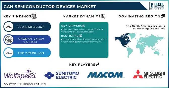
GaN Semiconductor Devices Market Size Analysis:
The GaN Semiconductor Devices Market Size was valued at USD 2.59 Billion in 2023 and expected to reach USD 18.68 Billion by 2032, and grow at a CAGR of 24.55% over the forecast period 2024-2032.
The GaN semiconductor devices market is experiencing rapid growth, primarily driven by the increasing demand for energy-efficient technologies across sectors such as power electronics, renewable energy, electric vehicles (EVs), and consumer electronics. GaN semiconductors offer superior energy efficiency compared to traditional silicon-based devices, which makes them ideal for high-performance applications. In the EV market, GaN plays a crucial role in EV battery chargers, DC/DC converters, traction inverters, and wireless charging systems, with significant improvements in efficiency, including up to 70% efficiency gains in inverters. The technology's ability to reduce the weight and size of power electronics by a third is boosting its adoption, especially in automotive and industrial applications. Additionally, GaN power devices are becoming essential for 5G technology, enhancing power efficiency for RF and power amplifiers.
Get more information on GaN Semiconductor Devices Market - Request Sample Report
A major trend driving market growth is the demand for faster charging speeds, with GaN chargers emerging as a key solution for mobile devices, offering higher efficiency and reduced charging times. Moreover, ammonia-free GaN production is gaining traction for its environmental benefits, improving crystal quality and positioning GaN as a more sustainable alternative to other semiconductors. Government initiatives promoting clean energy and renewable technologies are further accelerating GaN adoption, with applications in solar inverters, electric vehicle chargers, and wind turbines. As the demand for energy-efficient devices continues to rise, GaN semiconductors are poised to dominate various industries, cementing their position as a vital technology for sustainable growth. The market's expansion is further supported by the potential of gallium as a rare resource, with increasing focus on securing supply chains, recycling, and developing new sources. With these factors combined, the GaN semiconductor market is set for significant growth in the coming years.
GaN Semiconductor Devices Market Dynamics
Drivers
-
GaN Semiconductors as a Catalyst for Electric Vehicle Innovation and Sustainability
The rise in Electric Vehicle adoption is fueling the rapid growth of Gallium Nitride semiconductor devices, which are critical in enhancing the performance and efficiency of EVs. As the automotive industry transitions towards more sustainable and cost-effective alternatives to traditional combustion engine vehicles, the demand for high-performance power devices is growing. GaN semiconductors offer substantial advantages over silicon-based devices, including higher efficiency, reduced size, and lighter weight, making them ideal for key EV components such as inverters, battery chargers, and DC/DC converters. These advantages help optimize energy conversion, reduce charging times, and extend driving ranges. EVs are also gaining popularity due to their zero-emission nature, which contributes to a 50%-70% reduction in CO2 emissions compared to conventional vehicles. GaN technology is accelerating the electrification of vehicles, especially hybrid and fully electric models ability to manage high power densities efficiently. Testing by AVL has demonstrated that GaN-on-silicon semiconductors achieve over 99% efficiency, outperforming silicon carbide inverters by reducing energy losses by more than 60%.
Additionally, GaN’s lower production energy requirements compared to SiC make it a more ecologically friendly option. GaN semiconductors are manufactured in standard silicon semiconductor facilities, making them more scalable and cost-effective. As more companies invest in GaN technology to advance rapid charging solutions and enhance EV powertrains, the semiconductor market is expected to expand rapidly. This shift toward GaN-powered EV components positions GaN semiconductors as a key enabler of clean and efficient automotive power systems, driving technological innovation while meeting the growing demand for sustainable mobility solutions.
Restraints
-
Limited Availability of Raw Materials and Supply Chain Challenges for GaN Semiconductors
Gallium, a rare element, is essential in the production of Gallium Nitride semiconductors, and its scarcity could impact the scalability and cost-effectiveness of GaN production. As the demand for GaN-based power devices, particularly in sectors like electric vehicles, renewable energy, and telecommunications, continues to grow, the pressure on the supply chain is increasing. The current supply chain for gallium faces disruptions and inefficiencies, as its extraction and refinement are complex and resource-intensive. This can lead to price volatility and availability issues, which could hinder the rapid adoption of GaN technologies. Additionally, while alternatives such as Silicon Carbide semiconductors are being explored, GaN is still highly dependent on gallium for its production. Manufacturers may also face challenges in sourcing sufficient quantities of high-quality gallium, as the material is mainly produced as a byproduct of aluminum extraction. This supply chain vulnerability makes it difficult for companies to scale up GaN production in response to rising demand. Innovations in raw material sourcing and production techniques, such as ammonia-free GaN production, are underway to reduce environmental impact and improve crystal quality, but these solutions are still emerging and may not yet fully alleviate the raw material constraints.
GaN Semiconductor Devices Market Segment Outlook
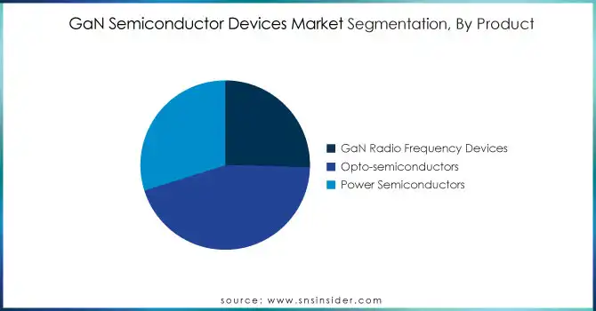
By Product
The opto-semiconductor segment holds a dominant share of around 45% in the GaN semiconductor devices market in 2023. Gallium Nitride is particularly well-suited for opto-electronic applications due to its ability to efficiently emit light across the visible and ultraviolet spectrums. GaN-based light-emitting diodes (LEDs) are widely used in energy-efficient lighting, displays, and automotive applications, offering superior brightness, color quality, and long lifespan compared to traditional LED technologies. Additionally, GaN-based laser diodes provide higher power output and energy efficiency, which is driving their adoption in optical communication systems, data storage, and advanced laser technologies. The demand for more energy-efficient and compact lighting solutions continues to propel growth in this segment.
By Component
The Power IC segment accounts for around 33% of the GaN semiconductor devices market in 2023, driven by the increasing demand for efficient power management solutions across various industries, including automotive, telecommunications, and consumer electronics. GaN-based power integrated circuits offer significant advantages over traditional silicon-based ICs, such as higher efficiency, faster switching speeds, and reduced power loss. These benefits make them ideal for use in power supplies, inverters, motor drives, and DC/DC converters, where high-performance power conversion is crucial. Additionally, GaN power ICs enable smaller, lighter designs and improved thermal management, contributing to the miniaturization of electronic devices. As industries move toward more compact and energy-efficient solutions, the power IC segment is poised for continued growth, particularly in electric vehicles and renewable energy systems.
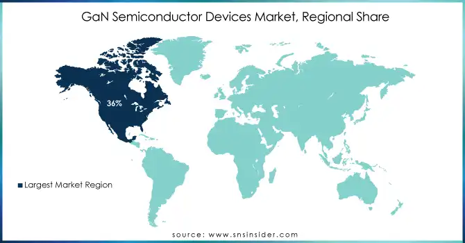
GaN Semiconductor Devices Market Regional Analysis:
In 2023, North America holds the largest share of around 36% in the GaN semiconductor devices market, driven by strong demand across various industries, including automotive, telecommunications, and consumer electronics. The region benefits from a robust technological infrastructure, significant investments in research and development, and the presence of leading semiconductor manufacturers. The growth of electric vehicle adoption and the increasing push for energy-efficient solutions are key drivers in North America, with GaN-based devices being essential for power management in EVs, renewable energy systems, and power supplies. Additionally, government initiatives promoting clean energy and sustainability further fuel the demand for GaN semiconductors. As a result, North America is expected to maintain its leadership in the global GaN market.
Asia-Pacific is the fastest-growing region in the GaN semiconductor devices market over the forecast period from 2024 to 2032, driven by rapid industrialization, technological advancements, and increasing demand for energy-efficient solutions. The region is home to major semiconductor manufacturing hubs, such as China, Japan, South Korea, and Taiwan, where leading companies are adopting GaN technology for power management in various applications, including electric vehicles, telecommunications, consumer electronics, and renewable energy. The expansion of the EV market in countries like China and Japan, coupled with the increasing adoption of 5G technology, is driving the demand for GaN-based devices. Additionally, supportive government policies, substantial investments in R&D, and growing manufacturing capabilities are accelerating the growth of the GaN semiconductor market in Asia-Pacific, positioning it as the leading region for market expansion.
Need any customization research on GaN Semiconductor Devices Market - Enquiry Now
GaN Semiconductor Devices Companies are:
Some of the major key players in GaN Semiconductor Devices with their product:
-
Wolfspeed, Inc. (GaN HEMT Transistors)
-
Sumitomo Electric Industries, Ltd. (GaN RF Devices)
-
MACOM Technology Solutions Holdings, Inc. (GaN Power Amplifiers)
-
Mitsubishi Electric Corporation (GaN Power Modules)
-
ROHM Co., Ltd. (GaN Power Devices)
-
STMicroelectronics N.V. (GaN Power Transistors)
-
Innoscience Technology (GaN-on-Si Power Devices)
-
Fujitsu Ltd. (GaN High Electron Mobility Transistors)
-
NexGen Power Systems (GaN Power ICs)
-
Odyssey Semiconductor Technologies, Inc. (GaN Power Switching Devices)
-
Panasonic Corporation (GaN Power Transistors)
-
Osram Opto Semiconductors GmbH (GaN-based LEDs)
-
Aixtron SE (GaN Epitaxial Equipment)
-
Koninklijke Philips N.V. (GaN Power Devices)
-
Taiwan Semiconductor Manufacturing Company (TSMC) (GaN Foundry Services)
-
Intel Corporation (GaN Power Amplifiers)
-
GLOBALFOUNDRIES (GaN RF Solutions)
-
Semiconductor Manufacturing International Corporation (SMIC) (GaN Power Electronics)
-
Skyworks Solutions, Inc. (GaN RF Amplifiers)
-
Analog Devices, Inc. (GaN Power Modules)
-
Efficient Power Conversion Corporation (GaN Power ICs)
-
Transphorm, Inc. (GaN Power Devices)
-
Infineon Technologies AG (GaN Power Solutions)
-
NXP Semiconductors (GaN Power Devices)
-
Qorvo, Inc. (GaN RF Amplifiers)
-
Texas Instruments Incorporated (GaN Power Devices)
-
Toshiba Corporation (GaN Power Devices)
-
GaN Systems (GaN Power Transistors)
-
NTT Advanced Technology Corporation (GaN Power Solutions)
List of key suppliers for raw materials and components used in the production of GaN (Gallium Nitride) semiconductor devices:
Raw Material Suppliers:
-
Sumitomo Chemical Co., Ltd. (Gallium)
-
Albemarle Corporation (Gallium Nitride)
-
Aurelius Technologies, Inc. (Gallium)
-
China National Petroleum Corporation (CNPC) (Gallium)
-
Praxair, Inc. (Nitrogen for GaN production)
-
Honeywell International Inc. (Silicon carbide (SiC) wafers for GaN devices)
-
Mitsubishi Chemical Corporation (Gallium and precursors for GaN synthesis)
-
Linde PLC (High-purity gases such as hydrogen and nitrogen)
-
Kyocera Corporation (Raw materials for GaN wafer substrates)
-
II-VI Incorporated (Silicon carbide and other substrate materials)
Component Suppliers:
-
Freescale Semiconductor (now part of NXP Semiconductors) (GaN-based power transistors)
-
Wolfspeed, Inc. (GaN HEMT (High Electron Mobility Transistor) components)
-
Transphorm, Inc. (GaN power devices)
-
Infineon Technologies AG (GaN power transistors and ICs)
-
GaN Systems Inc. (GaN power devices and power modules)
-
Macom Technology Solutions Inc. (GaN RF devices)
-
STMicroelectronics (GaN power devices and transistors)
-
Qorvo, Inc. (GaN RF power amplifiers)
-
Rohm Semiconductor Co., Ltd. (GaN power devices)
-
Texas Instruments (GaN power ICs)
Recent Development
-
March 2024, EPC has introduced the EPC2361, a 100V GaN FET with an ultra-low 1mΩ on-resistance, offering double the power density compared to previous models. This new FET improves power conversion efficiency, reducing energy consumption and heat dissipation, and is ideal for high-power applications such as AC–DC synchronous rectification and eMobility. The EPC2361 is priced at $4.60 each in 3 Ku volumes.
-
January, 2024, Transphorm has introduced two new SuperGaN® FETs in a 4-lead TO-247 package, the TP65H035G4YS and TP65H050G4YS, offering on-resistances of 35mOhm and 50mOhm, respectively. These devices provide versatility for high-power applications in data centers, renewable energy, and industrial power conversion, reducing losses by up to 27% compared to SiC MOSFETs.
| Report Attributes | Details |
| Market Size in 2023 | USD 2.59 Billion |
| Market Size by 2032 | USD 18.68 Billion |
| CAGR | CAGR of 24.55% From 2024 to 2032 |
| Base Year | 2023 |
| Forecast Period | 2024-2032 |
| Historical Data | 2020-2022 |
| Report Scope & Coverage | Market Size, Segments Analysis, Competitive Landscape, Regional Analysis, DROC & SWOT Analysis, Forecast Outlook |
| Key Segments | • By Product (GaN Radio Frequency Devices, Opto-semiconductors, Power Semiconductors) • By Component (Power IC, Transistor, Rectifier, Diode, Others) • By Wafer Size (2-inch, 4-inch, 6-inch, 8-inch) • By Application (Signal, Power, Communications, Consumer Electronics, Automotive, Military & Defense, Medical, Lighting and Lasers, Supplies and Inverters, Radio Frequency, Other) |
| Regional Analysis/Coverage | North America (US, Canada, Mexico), Europe (Eastern Europe [Poland, Romania, Hungary, Turkey, Rest of Eastern Europe] Western Europe] Germany, France, UK, Italy, Spain, Netherlands, Switzerland, Austria, Rest of Western Europe]), Asia Pacific (China, India, Japan, South Korea, Vietnam, Singapore, Australia, Rest of Asia Pacific), Middle East & Africa (Middle East [UAE, Egypt, Saudi Arabia, Qatar, Rest of Middle East], Africa [Nigeria, South Africa, Rest of Africa], Latin America (Brazil, Argentina, Colombia, Rest of Latin America) |
| Company Profiles | Wolfspeed, Inc., Sumitomo Electric Industries, Ltd., MACOM Technology Solutions Holdings, Inc., Mitsubishi Electric Corporation, ROHM Co., Ltd., STMicroelectronics N.V., Innoscience Technology, Fujitsu Ltd., NexGen Power Systems, Odyssey Semiconductor Technologies, Inc., Panasonic Corporation, Osram Opto Semiconductors GmbH, Aixtron SE, Koninklijke Philips N.V., Taiwan Semiconductor Manufacturing Company (TSMC), Intel Corporation, GLOBALFOUNDRIES, Semiconductor Manufacturing International Corporation (SMIC), Skyworks Solutions, Inc., Analog Devices, Inc. |
| Key Drivers | • GaN Semiconductors as a Catalyst for Electric Vehicle Innovation and Sustainability. |
| Restraints | • Limited Availability of Raw Materials and Supply Chain Challenges for GaN Semiconductors. |
Get in Touch
