EUV Pellicle Market Report Scope & Overview:
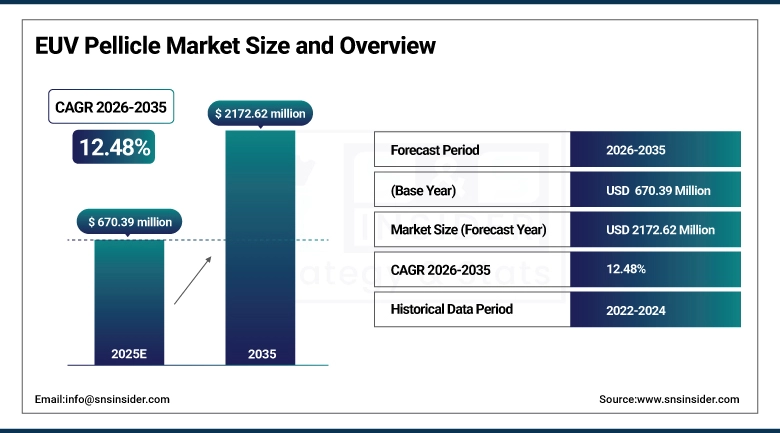
The EUV Pellicle Market size was valued at USD 670.39 Million in 2025 and is projected to reach USD 2172.62 Million by 2035, growing at a CAGR of 12.48% during 2026–2035.
The Extreme Ultraviolet (EUV) pellicle market is gaining traction as a result of the rising demand for high-precision inspection and advanced production technologies within the EUV manufacturing processes. New inspection tools promote quality control by maxing pellicles to high gravity EUV radiation and thermal shock pulses but keeping their optical transparencies. This leads to improved wafer yields and more effective semiconductor fabrication. With in-house manufacturing processes and advanced materials, manufacturers can achieve superior quality, lower dependency on supply chains and faster process integration. These durability enhancements, inspection accuracy, and scalable production solutions provide a compelling value proposition to market adoption, next generation semiconductor nodes and ultimately the sustainable technology and commerce evolution of the EUV pellicle segment.
In September 2025, Skytech Inc will be first out of the gate in commercial PVD equipment with an order due in Sep 2025 that will play a key role in leading adoption of fan-out panel-level packaging (PLP) technology, bringing better AI chip capacity.
Market Size and Forecast:
-
Market Size in 2025: USD 670.39 Million
-
Market Size by 2035: USD 2172.62 Million
-
CAGR: 12.48% from 2026 to 2035
-
Base Year: 2025
-
Forecast Period: 2026–2035
-
Historical Data: 2022–2024
To Get more information on EUV Pellicle Market - Request Free Sample Report
EUV Pellicle Market Highlights:
-
The EUV pellicle market is driven by increasing in-house production to improve cost efficiency, supply reliability, and process performance.
-
Advanced materials like carbon nanotube membranes enhance pellicle durability and optical transparency, boosting wafer yields.
-
Manufacturers are investing in next-generation EUV pellicle technologies to support ultra-fine semiconductor nodes and accelerate commercialization.
-
Technical and supply chain challenges, including high production costs and dependence on specialized materials, restrain widespread adoption.
-
Strategic collaborations and investments in innovative startups are creating growth opportunities and encouraging technological self-reliance.
-
Leading players, such as TSMC and Samsung Foundry, are internalizing pellicle production to secure supply chains and strengthen competitive advantages.
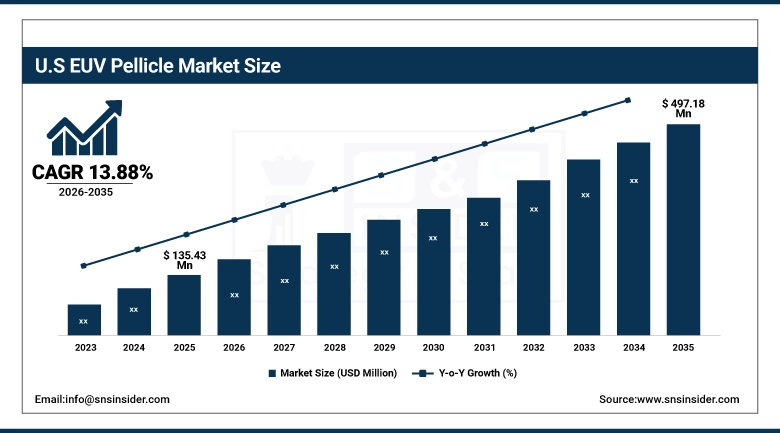
U.S. Extreme Ultraviolet (EUV) Pellicle Market Size Outlook:
The U.S. Extreme Ultraviolet (EUV) Pellicle Market was valued at USD 135.43 Million in 2025 and is projected to reach USD 497.18 Million by 2035, growing at a CAGR of 13.88% during 2026–2035. Growing industry initiatives to establish in-house manufacturing, coupled with advanced material developments resulting in pellicles that are more durable, optically transparent, and capable of generating higher wafer yields, while reducing supply chain dependencies and process efficiencies, are driving the market.
Market Drivers: In-House Production Driving Cost Efficiency and Reliability in EUV Pellicle Market
Increasing trend of manufacturers towards in-house production to improve cost-effectiveness, supply reliability, and overall process performance is estimated to drive the demand for EUV pellicle market over the forecast period. Considering that EUV pellicles require replacement with high frequency, internally controlling the manufacturing enables better quality control, eliminates the dependency on third-party suppliers and assures constant availability. New material advances for example, carbon nanotube membranes provide non-embrittled, non-blocking optical transparency as well as robust durability of materials that further improve wafer yields and process efficiency. These endeavors together catalyze market expansion by driving adoption of advanced EUV pellicles, sustainable for next-gen semiconductor nodes and bolstering differentiation for leading players.
In Sept 2025, TSMC is shifting its old 8-inch Fab 3 in Sept 2025 to produce the EUV pellicles in-house, in-order to eliminate excessive costs, ensure predictable supply, and enhance the wafer yield benefiting from integrated pellicle repair for high durability and lifetime pellicle to be integrated with excellent optical performance.
Market Restraints: Technical and Supply Chain Constraints Limiting Extreme Ultraviolet (EUV) Pellicle Market Growth
The EUV pellicle market is hampered by technical and operational hurdles. Challenges include high production costs and complicated manufacturing process for mass adoption, but the most difficult technical hurdle is overcoming adequate transmittance and durability. Dependence on niche material and niche equipment makes the supply chain more fragile and leads to delays and increased operational risk. EUV pellicles are particularly tricky to scale because of the stringent quality standards. All of these factors, collectively, restrain the market size and slow the market growth potential by making market entry hard for new players and leading to less innovation, in turn, affecting the overall growth potential of the EUV pellicle market.
Market Opportunities: Strategic In-House Development Driving EUV Pellicle Industry Expansion
There are significant growth opportunities in EUV pellicle market as semiconductor manufacturers set their sights on bringing development and technological self-reliance in-house. Response With the tackiness of wafer transmittance throughout the wafer manufacturing process, the increased demand for ultra-fine semiconductor manufacturing is driving companies to research and develop new advanced pellicle technologies that can achieve high levels of transmittance, greater pellicle durability and higher overall process efficiency. This shift promote diversification, decreasing reliance on external establishments via nearby summarize channels, and continues to streamline the commercialization of the EUV solutions. Investments alongside these unique startups and tech partners substantially increase the addressable market, Due to the increasing focus on high-performance, reliable EUV pellicles, the market is poised to continue to grow and innovate.
In Feb 2025, Samsung Foundry is preparing to launch its own EUV pellicles but is also investing in Korean companies, including S&S Tech and FST, to diversify the supply chain to make supply more stable while also securing independent tech when they commercialize in Feb 2025.
EUV Pellicle Market Segment Highlights:
-
By Product Type: Dominant – Membrane Pellicles (59.88% in 2025 → 59.13% in 2035); Fastest-Growing – Non-Membrane Pellicles (CAGR 12.74%)
-
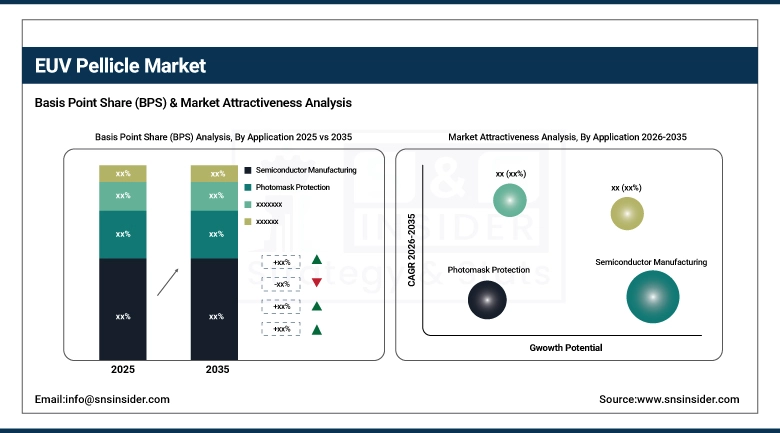
By Application: Dominant – Semiconductor Manufacturing (50.00% in 2025 → 45.00% in 2035); Fastest-Growing – Photomask Protection (CAGR 13.54%)
-
By End User: Dominant – Foundries (50.50% in 2025 → 53.50% in 2035); Fastest-Growing – Foundries (CAGR 13.29%)
-
By Distribution Channel: Dominant – Direct Sales (54.25% in 2025 → 49.75% in 2035); Fastest-Growing – OEM Partnerships (CAGR 14.92%)
By Application, Semiconductor Manufacturing Dominating and Photomask Protection Fastest-Growing
Semiconductor Manufacturing remains the dominant application in both 2025 and 2035, holding the largest market share due to its critical role in wafer fabrication and lithography processes. Photomask Protection Is the Fastest-Growing Application as there is a rising requirement for advance protection solution that helps to increase the photomask lifetime and production efficiency.
By Product Type, Membrane Pellicles Dominating and Non-Membrane Pellicles Fastest-Growing
Membrane Pellicles remain the dominant product type in both 2025 and 2035, accounting for the largest market share due to their high durability, optical clarity, and widespread use in semiconductor lithography. Non-Membrane Pellicles is expected to grow at the fastest pace owing to increasing need for superior pellicle solutions compatible with EUV lithography, mass production, and economical protection of wafers.
By End User, Foundries Dominating and Fastest-Growing
Foundries continue to dominate the market in both 2025 and 2035, capturing the largest share due to their central role in semiconductor production. They are also the fastest-growing end user segment, fueled by rising investments in high-volume manufacturing, EUV adoption, and advanced wafer processing capabilities.
By Distribution Channel, Direct Sales Dominating and OEM Partnerships Fastest-Growing
Direct Sales remain the dominant distribution channel from 2025 to 2035, supported by strong manufacturer-client relationships and streamlined supply chains. OEM Partnerships are the quickest to grow channel as a result of professional associations, co-development projects, and the corresponding increase in interest in integrated pellicle systems.
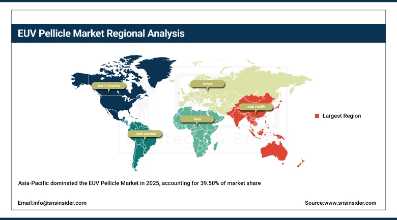
Extreme Ultraviolet (EUV) Pellicle Market Regional Highlights:
-
Asia-Pacific: In 2025 39.50% → 36.50% in 2035, Dominating Region, Moderate Decline (CAGR 11.36%)
-
North America: In 2025 30.63% → 35.31% in 2035, Significant Market, Fastest Growth (CAGR 14.08%)
-
Europe: In 2025 19.88% → 18.94% in 2035, Mature Market, Slight Decline (CAGR 11.94%)
-
South America: In 2025 5.13% → 6.06% in 2035, Emerging Market, Strong Growth (CAGR 14.37%)
-
Middle East & Africa: In 2025 4.88% → 3.94% in 2035, Developing Market, Moderate Decline (CAGR 10.08%)
Asia-Pacific EUV Pellicle Market Insights:
The Asia-Pacific region continues to drive the largest share of the EUV Pellicle market due to an established semiconductor manufacturing base, rapid adoption of advanced lithography technologies, and high expenditure on wafer fabrication facilities or front-end semiconductor manufacturing. The region will continue to dominate the market for the above-mentioned reasons along with higher foundry demand and expansion in production capabilities.
Get Customized Report as per Your Business Requirement - Enquiry Now
China EUV Pellicle Market Insights:
There are several reasons behind the dominance of China for EUV Pellicle, as the country continues to grow semiconductor manufacturing sector, investments in advanced lithography technologies are increasing, and hence are the demands for high-volume wafer fabrication and photomask protection solutions.
North America EUV Pellicle Market Insights:
Due to an increase in semiconductor fabrication investments, the growth of advanced EUV lithography technologies, and the alliances formed between manufacturers and foundries, North America is the fastest-growing region in the EUV Pellicle industry. Besides, due to robust R&D activities and surging demand for high-precision photomask protection also propels the regional market growth.
U.S. EUV Pellicle Market Insights:
The U.S. dominates the North America EUV Pellicle market, supported by its advanced semiconductor industry, high adoption of EUV lithography, and strong investments in wafer fabrication and photomask protection technologies.
Europe EUV Pellicle Market Insights:
There is an emerging trend in the Europe EUV Pellicles market pertaining to the evolving shifts towards the adoption of higher advanced lithography technologies, growing government support for the semiconductor manufacturing, increasing investments in R&D. Enabling Trends: The above-mentioned factors are shaping the evolving landscape of the photomask market in the region.
Germany EUV Pellicle Market Insights:
Germany dominates the EUV Pellicle market, driven by its strong semiconductor manufacturing infrastructure, advanced lithography capabilities, and robust R&D initiatives. High demand for precision photomask protection and strategic industry collaborations further reinforce Germany’s leadership in the regional market.
Latin America EUV Pellicle Market Insights:
The Latin America Extreme Ultraviolet Pellicle Market is slowly growing mainly due to growing investment in semiconductor fabrication, increasing adoption of advanced lithography technologies within these industrial hubs paired with growing demand for photomask protection solutions.
Brazil EUV Pellicle Market Insights:
Brazil is the dominant country in the Latin America EUV Pellicle industry, driven by its leading semiconductor manufacturing activities, growing industrial investments, and increasing demand for advanced lithography and photomask protection solutions.
Middle East & Africa EUV Pellicle Market Insights:
The Middle East and Africa EUV Pellicle Industry is currently experiencing steady growth, driven by growing investment into semiconductor production, adoption of high-end lithography technologies, and increasing requirement for photomask protection solutions. Across the region, stable market growth is also supported due to strategic partnerships and initiatives supported by the government strengthening technological development.
Saudi Arabia EUV Pellicle Market Insights:
Saudi Arabia is the dominant country in the Middle East and Africa EUV Pellicle Industry, owing to its investments in semiconductor infrastructure, technology adoption initiatives and increasing demand for advanced lithography and photomask protection solutions in the country.
EUV Pellicle Market Competitive Landscape:
Mitsui Chemicals, Inc. (Tokyo: 4183) is a global chemical company specializing in advanced materials, performance products, and life science solutions. With expertise in polymers, coatings, and semiconductor materials, it develops innovative technologies like EUV pellicles, supporting electronics, automotive, healthcare, and sustainability initiatives worldwide while driving industrial and technological advancements.
-
In May 2024, Mitsui Chemicals announced the establishment of production facilities at Iwakuni-Ohtake Works for next-generation CNT EUV pellicles, enhancing semiconductor performance and productivity with high transmittance and durability.
TOPPAN Inc., established in 1900, is a global technology company specializing in printing, electronics, and semiconductor solutions. It develops advanced photomasks, FC-BGA substrates, and packaging technologies for high-performance semiconductors, supporting AI, data centers, and next-generation EUV processes, while driving innovation in electronics manufacturing and smart applications worldwide.
-
In Dec 2025, TOPPAN and Tekscend Photomask showcased advanced semiconductor photomasks, FC-BGA substrates, and next-generation EUV-supporting technologies at SEMICON Japan 2025, highlighting expanded production capacity and development for AI, data center demand, and high-performance semiconductor packaging.
EUV Pellicle Companies are:
-
Toppan Photomasks, Inc
-
Shin-Etsu Chemical Co., Ltd
-
Mitsui Chemicals, Inc
-
Nippon Kayaku Co., Ltd
-
S&S Tech Co., Ltd
-
SKC Co., Ltd
-
LG Chem Ltd
-
Sumitomo Chemical Co., Ltd
-
Tokyo Electron Limited
-
Lam Research Corporation
-
Applied Materials, Inc
-
KLA Corporation
-
Samsung Electronics Co., Ltd
-
Intel Corporation
-
Taiwan Semiconductor Manufacturing Company Limited (TSMC)
-
GlobalFoundries Inc
-
Canon Inc
-
Nikon Corporation
| Report Attributes | Details |
|---|---|
| Market Size in 2025 | USD 670.39 Million |
| Market Size by 2035 | USD 2172.62 Million |
| CAGR | CAGR of 12.48% From 2026 to 2035 |
| Base Year | 2025 |
| Forecast Period | 2026-2035 |
| Historical Data | 2022-2024 |
| Report Scope & Coverage | Market Size, Segments Analysis, Competitive Landscape, Regional Analysis, DROC & SWOT Analysis, Forecast Outlook |
| Key Segments | • By Product Type(Membrane Pellicles and Non-Membrane Pellicles) • By Application(Semiconductor Manufacturing, Photomask Protection and Others) • By End User(Integrated Device Manufacturers, Foundries and Others) • By Distribution Channel(Direct Sales, Distributors & Resellers, OEM Partnerships and Online/Platform Sales) |
| Regional Analysis/Coverage | North America (US, Canada), Europe (Germany, UK, France, Italy, Spain, Russia, Poland, Rest of Europe), Asia Pacific (China, India, Japan, South Korea, Australia, ASEAN Countries, Rest of Asia Pacific), Middle East & Africa (UAE, Saudi Arabia, Qatar, South Africa, Rest of Middle East & Africa), Latin America (Brazil, Argentina, Mexico, Colombia, Rest of Latin America). |
| Company Profiles | ASML Holding N.V., Toppan Photomasks, Inc., Shin-Etsu Chemical Co., Ltd., Mitsui Chemicals, Inc., Nippon Kayaku Co., Ltd., S&S Tech Co., Ltd., Entegris, Inc., SKC Co., Ltd., LG Chem Ltd., Sumitomo Chemical Co., Ltd., Tokyo Electron Limited, Lam Research Corporation, Applied Materials, Inc., KLA Corporation, Samsung Electronics Co., Ltd., Intel Corporation, Taiwan Semiconductor Manufacturing Company Limited (TSMC), GlobalFoundries Inc., Canon Inc., Nikon Corporation. |
Get in Touch
