Nanopatterning Market Report Scope & Overview:
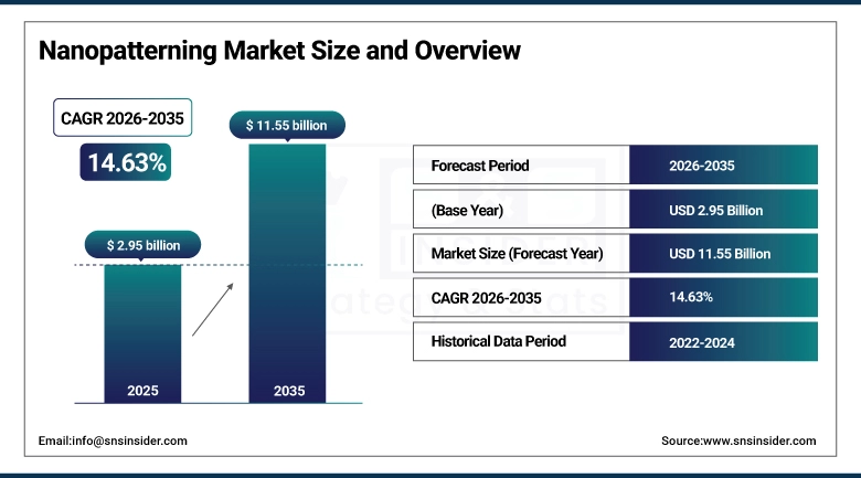
The Nanopatterning Market size was valued at USD 2.95 Billion in 2025 and is projected to reach USD 11.55 Billion by 2035, growing at a CAGR of 14.63% during 2026–2035.
Increased demand for miniaturization of electronic components, high-performance devices, and advanced semiconductor devices is sustaining growth in the nanopatterning market. The growing usage of nanoscale fabrication technologies (for example, lithography, nanoimprint, and laser-based patterning) is facilitating manufacturing processes with enhanced precision, scalability, and efficiency. In addition, rising applications within photonics, optical communication, healthcare, and semiconductor packaging are also contributing towards market growth. Technological improvements and continuous investment towards R&D ongoing, make process accuracy and throughput higher. Furthermore, with the recent dawn of new fourth industrial revolution technologies like quantum computing, electronic skin, and advanced sensors, nanopatterning has become an enabling technology that underpins modern and future industrial applications.
In January 2026, Nanoscribe unveiled its Shanghai Quantum X demolab capable of sub-200-nanometer resolution two-photon lithography for high-accuracy nanopatterning and 3D microfabrication. The facility features scalable, high-precision fabrication workflows for photonic integrated circuits fabrication for applications in photonics, semiconductor packaging and optical communication technologies.
Nanopatterning Market Size and Growth Forecast:
-
Market Size in 2025: USD 2.95 Billion
-
Market Size by 2035: USD 11.55 Billion
-
CAGR: 14.63% during 2026–2035
-
Base Year: 2025
-
Forecast Period: 2026–2035
-
Historical Data: 2022–2024
To Get more information on Nanopatterning Market - Request Free Sample Report
Nanopatterning Market Trends Highlights:
-
Increasing demand for miniaturized and high-performance electronic devices driving adoption of advanced nanopatterning techniques
-
Rapid advancements in lithography, nanoimprint, and laser-based fabrication improving precision, scalability, and efficiency
-
Expanding applications across semiconductors, photonics, optical communication, and healthcare sectors
-
Growing investments in research and development supporting innovation in nanoscale manufacturing technologies
-
Rising importance of nanopatterning in quantum computing, flexible electronics, and next-generation sensors
-
Increasing focus on cost-effective, high-throughput, and maskless fabrication methods enhancing commercial viability
U.S. Nanopatterning Market Size Outlook:
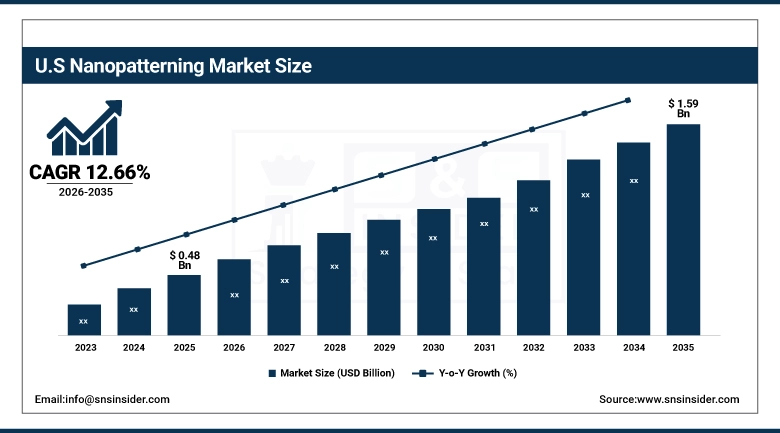
The U.S. Nanopatterning Market was valued at USD 0.48 Billion in 2025 and is projected to reach USD 1.59 Billion by 2035, growing at a CAGR of 12.66% during 2026–2035, due to rising adoption of advanced semiconductor manufacturing, miniaturized electronic devices, and high-performance photonic components. Supporting market growth is increasing utilization of nanotechnology in health care, quantum computing, and flexible electronics. In the meantime, ongoing R&D investment as well as progress in lithography and scalable fabrication techniques are improving precision, efficiency, and the ability to scale production while also driving overall market growth.
Nanopatterning Market Drivers:
-
Advancements in Scalable and High-Precision Nanofabrication Technologies
The nanopatterning market is driven by the continuous advancement of nanofabrication techniques such as lithography, self-assembly, and laser-based nanopatterning. They provide precise nanoscale control, which can benefit the realization of novel semiconductors, photonic devices, and biomedical applications. As the need for ever-tinier, higher-performing electronic components grows, manufacturers are turning to advanced nanopatterning methods that enhance resolution, repeatability, and efficiency. Moreover, maskless fabrication, decrease of material wastage b, and usage of many different types of substrates are improving production scalability. Increasing R&D investments coupled with the growing applications in the field of quantum computing, flexible electronics, and advanced sensors are propelling the growth and adoption of the market globally.
In November 2024 Light-driven nanopatterning aids the self-assembly of semiconductor nanoparticles using surface charge modulation based on UV-induced ligand cleavage, alleviating the need for sophisticated optical setups. Such scalable and economical approach enables uniform nanoscale patterning with implications for UV detectors, flexible electronics, and smart microdevices.
Nanopatterning Market Restraints:
-
High Costs and Technical Complexity Limiting Nanopatterning Adoption
The nanopatterning market is primarily restrained due to high equipment costs, complexity of nanopatterning processes and fabrication techniques, and the requirement for specialized infrastructural facilities. The capital costs associated with advanced lithography systems and nanofabrication tools makes uptake difficult for small and mid-sized enterprises. Moreover, it requires high-controlled environments, high-skilled workforces, and tight process conditions to sustain accuracy at the nanoscale level, so it adds complexity to the operations as well. Material restrictions, low throughput in some techniques, as well as scalability issues limit mass commercialization. The emerging nanopatterning technologies have high demand potential across multiple industries but are currently limited in rapid adoption by integration issues with existing semiconductor manufacturing workflows and slow standardization.
Nanopatterning Market Opportunities:
-
Scalable Nano-OLED Fabrication and Advanced Lithography Growth
There are several lucrative opportunities in the nanopatterning market propelled by increasing need for highly precise, high-resolution displays and miniaturization of electronic components, particularly transmission photonic and optoelectronic devices which are driving new material innovations. This could improve efficiency and functionality in a variety of sectors AR/VR, micro-displays, integrated photonics, etc. based on sub-diffraction-limit fabrication with innovations in different devices. Finally, cost-effective, scalable and resist-free lithography methods are paving the way to an efficient manufacturing scale. Also, growing funding for nanotechnology research and development, along with rising utilization in semiconductors, medical devices, and metasurfaces, is anticipated to fuel commercialization and expand the application range of nanopatterning technologies across various sector.
In Dec 2025, Scalable nano-OLED nanopatterning is the dominant approach due to its ability to fabricate sub-diffraction-limit devices with high pixel density and precise nanoscale control, while resist-free self-aligned lithography is the fastest-growing method driven by scalability, high resolution, and increasing applications in advanced displays and photonics.
Nanopatterning Market Segment Highlights:
-
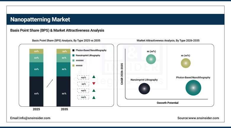
By Type: Dominant – Photon-Based Nanolithography (69.00% → 61.00%, CAGR -13.22%); Fastest-Growing – Photon-Based Nanolithography (5.10% → 5.90%, CAGR -16.30%)
-
By Application: Dominant – Consumer Electronics (39.10% → 31.90%, CAGR -12.30%); Fastest-Growing – Healthcare (30.50% → 34.50%, CAGR -16.04%)
-
By Component: Dominant – Lithography Equipment (34.50% → 30.50%, CAGR -13.22%); Fastest-Growing – Light Sources (10.20% → 11.80%, CAGR -16.30%)
-
By End-User: Dominant – Foundries (39.80% → 40.00%, CAGR - 14.69%); Fastest-Growing – Semiconductor Manufacturers (25.30%→ 29.53%, CAGR -16.40%)
By Type: Photon-Based Nanolithography Dominant and Fastest-Growing
Photon-Based Nanolithography is estimated to account for the largest share of the nanopatterning market over the forecast period, owing to its greater penetration in the semiconductor fabrication and high-precision markets, and the segment is expected to grow the fastest, fueled by emerging nanopatterning methodology, growth in research and development funding, and growth in niche application sectors.
By Application: Consumer Electronics Dominant; Healthcare Fastest-Growing
The consumer electronics application segment accounts for the largest share of nanopatterning market owing to the high demand for miniaturized devices and high demand for smart phones, smart electronics components, etc. On the other hand, the healthcare segment is the fastest growing segment only second to consumer electronics on account of burgeoning demand for nanotechnology in diagnostics, medical devices, and biomaterials or biomedical research.
By Component: Lithography Equipment Dominant; Light Sources Fastest-Growing
The lithography equipment segment dominates in terms of value, as it is a key enabling technology that is imperative for high precision nanopatterning and semiconductor manufacturing; however, light sources are the fastest-growing segment driven by favorable developments in laser technologies and increasing demand for high-resolution patterning systems.
By End-User: Foundries Dominant; Semiconductor Manufacturers Fastest-Growing
Foundries are the dominant end-user segment due to large-scale semiconductor production and outsourcing trends, while semiconductor manufacturers are the fastest-growing segment driven by increasing in-house fabrication capabilities, rising chip demand, and expansion of advanced manufacturing facilities.
Nanopatterning Market Regional Highlights:
-
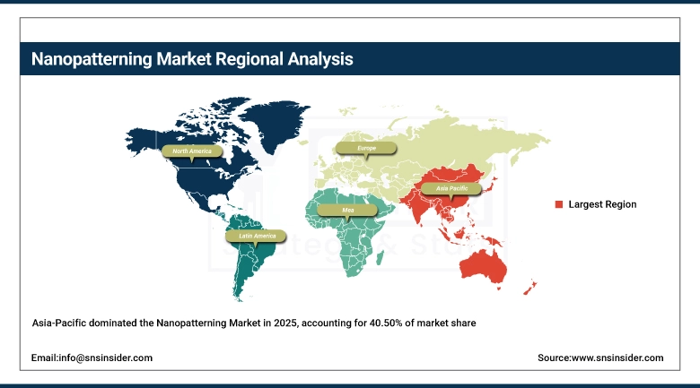
North America: 24.70% (2025) → 22.30% (2035), Dominant Region with strong semiconductor ecosystem, advanced R&D capabilities, and high adoption of nanopatterning in electronics, photonics, and advanced packaging applications (CAGR 13.46%)
-
Europe: 19.80% (2025) → 18.20% (2035), Mature Growth Region supported by strong research institutions, nanotechnology initiatives, and adoption across semiconductor manufacturing, MEMS, and precision engineering (CAGR 13.66%)
-
Asia-Pacific: 40.50% (2025) → 44.50% (2035), Fastest-Growing and Dominant Region driven by large-scale semiconductor manufacturing, strong electronics production base, and increasing investments in nanofabrication technologies (CAGR 15.71%)
-
South America: 7.90% (2025) → 7.10% (2035), Stable Region with gradual growth supported by rising R&D activities, limited but expanding semiconductor ecosystem, and increasing adoption of advanced technologies (CAGR 13.41%)
-
Middle East & Africa: 7.10% (2025) → 7.90% (2035), Emerging Growth Region driven by diversification initiatives, smart infrastructure projects, and increasing investments in advanced technology and nanotechnology applications (CAGR 15.85%)
Asia-Pacific Nanopatterning Market Insights:
Asia-Pacific captures the highest share of Nanopatterning market owing to the availability of semiconductor manufacturing hubs in countries like China, Japan, South Korea and Taiwan, supported by rapid industrialization and high investments in advanced fabrication technologies. The region's adoption and production capabilities are further strengthened by rising consumer electronics demand, expansion of foundries, and government support for nanotechnology R&D.
Get Customized Report as per Your Business Requirement - Enquiry Now
China Nanopatterning Market Insights:
China dominates the Nanopatterning Market, powered by high semiconductor manufacturing base, growing electronics industry, huge government investments in nanotechnology, and swift adoption of new fabrication and lithography technologies.
North America Nanopatterning Market Insights:
Nanopatterning Market in position for strong growth emanating from strong R&D investments, advanced semiconductor manufacturing infrastructure and presence of major technology players. Rapid growth in the application of nanotechnology due to innovations along with government financing in sectors such as electronics, healthcare and photonics that will boost the growth of the nanotech market throughout the U.S. and Canada.
United States Nanopatterning Market Insights:
The United States Nanopatterning market is growing steadily due to strong semiconductor R&D, increasing investments in advanced manufacturing, rising demand for nanotechnology in electronics and healthcare, and continuous innovation supported by leading technology firms and research institutions.
Europe Nanopatterning Market Insights:
Europe Nanopatterning market is currently growing moderately, supported by strong research institutions, government-backed nanotechnology initiatives, and the presence of key equipment manufacturers across Germany, France, and the Nordic region. Increasing adoption in semiconductor fabrication, photonics, and advanced materials, along with collaborations between academia and industry, is driving steady demand, although slower industrial scaling compared to Asia-Pacific tempers overall growth momentum.
Germany Nanopatterning Market Insights:
The Germany Nanopatterning market is expanding steadily, driven by rising semiconductor demand, miniaturization of electronic devices, growth in photonics and MEMS applications, increased R&D investments, and advancements in lithography technologies enabling high-precision nanoscale fabrication.
Latin America Nanopatterning Market Insights:
The Latin America Nanopatterning market is witnessing steady growth, due to increasing investments in research and development, gradual expansion of semiconductor and electronics manufacturing, and rising adoption of advanced nanotechnology in healthcare and industrial applications. Government initiatives to strengthen technological capabilities, along with growing collaborations with global players and academic institutions, are further supporting market development across key countries in the region.
Brazil Nanopatterning Market Insights:
The Brazil Nanopatterning market leads Latin America Latin America due to growing investments in research and development, expanding electronics and semiconductor activities, increasing adoption of nanotechnology in healthcare and industrial applications, and rising collaborations with global technology providers and academic institutions.
Middle East & Africa (MEA) Nanopatterning Market Insights:
The Middle East & Africa Nanopatterning market is also gradually expanding with investments in advanced technologies, increased focus on semiconductor diversification, and enhancing adoption of nanotechnology in various sectors including health care, energy, and telecommunications. Along with such government-backed innovation ecosystem enhancement, partnerships with global research organizations and technology vendors further amplify their local infrastructure and help stimulate wider regional uptake of nanopatterning solutions.
United Arab Emirates Nanopatterning Market Insights:
The United Arab Emirates Nanopatterning market is dominant, due to strong government support for advanced technologies, significant investments in research and innovation, rapid growth in semiconductor-related activities, and increasing adoption of nanotechnology across healthcare, energy, and smart infrastructure sectors.
Nanopatterning Market Competitive Landscape:
Heidelberg Instruments Mikrotechnik GmbH, a German company founded in 1984, integrates micro- and nanolithography systems, ranging from laser lithography, through maskless patterning, to nanoimprint solutions. Nanoscale device development and advanced material structuring — It serves semiconductor, photonics and research industries with high-precision fabrication equipment. The company is known for its innovative spirit, reliability, and collaborative research projects.
-
In Oct 2024, Heidelberg Instruments launched its NanoFrazor nanolithography system in, featuring modular architecture, up to 10× faster throughput, and advanced nanopatterning using t-SPL and DLS technologies. The system enables high-precision fabrication with resolutions down to 15 nm lateral and 2 nm vertical, supporting applications in quantum devices, nanophotonics, and nanoscale electronics.
SUSS MicroTec SE is a 1949 Germany-based semiconductor equipment company and provides lithography systems, wafer bonding and advanced packaging solutions. Meld Technology The technology supports mid-end and back-end semiconductor manufacturing processes for applications such as MEMS, power devices and heterogeneous integration. Its capabilities include high-precision tools that are critical for wafer-level production and advanced device fabrication, as well as scalable nanopatterning technologies and process solutions.
-
In Jan 2026, SUSS MicroTec SE reported that it is strengthening its position in the semiconductor industry by focusing on mid-end manufacturing solutions, including lithography, wafer bonding, and advanced packaging tools that support heterogeneous integration, MEMS, and specialty devices. The company’s technologies enable flexible, high-precision patterning and bonding processes essential for wafer-level optics, power electronics, and next-generation 3D integrated devices.
Nanopatterning Companies are:
-
EV Group (EVG)
-
SUSS MicroTec SE
-
Nanonex Corporation
-
NIL Technology ApS
-
Obducat AB
-
Vistec Electron Beam GmbH
-
SVG Optronics Co., Ltd.
-
Toppan Photomasks, Inc.
-
Nanoscribe GmbH
-
Raith GmbH
-
SET Corporation SA
-
IMS Chips
-
Nano-Terra, Inc.
-
NanoOpto Corporation
-
PROFACTOR GmbH
-
Canon Inc.
-
Nikon Corporation
-
Heidelberg Instruments Mikrotechnik GmbH
| Report Attributes | Details |
|---|---|
| Market Size in 2025 | USD 2.95 Billion |
| Market Size by 2035 | USD 11.55 Billion |
| CAGR | CAGR of 14.63% From 2026 to 2035 |
| Base Year | 2025 |
| Forecast Period | 2026-2035 |
| Historical Data | 2022-2024 |
| Report Scope & Coverage | Market Size, Segments Analysis, Competitive Landscape, Regional Analysis, DROC & SWOT Analysis, Forecast Outlook |
| Key Segments | • By Type (Nanoimprint Lithography, E-Beam Lithography, Photon-Based Nanolithography and Others) • By Application (Healthcare, Organic Devices, Consumer Electronics and Others) • By Component (Resists & Materials, Lithography Equipment, Masks & Templates, Light Sources and Others) • By End-User (Semiconductor Manufacturers, Research Institutes, Foundries, Original Equipment Manufacturers (OEMs) and Others) |
| Regional Analysis/Coverage | North America (US, Canada), Europe (Germany, UK, France, Italy, Spain, Russia, Poland, Rest of Europe), Asia Pacific (China, India, Japan, South Korea, Australia, ASEAN Countries, Rest of Asia Pacific), Middle East & Africa (UAE, Saudi Arabia, Qatar, South Africa, Rest of Middle East & Africa), Latin America (Brazil, Argentina, Mexico, Colombia, Rest of Latin America). |
| Company Profiles | EV Group (EVG); SUSS MicroTec SE; Raith GmbH; Heidelberg Instruments Mikrotechnik GmbH; Canon Inc.; Nikon Corporation; Nanoscribe GmbH; Obducat AB; NIL Technology ApS; Vistec Electron Beam GmbH; AMO GmbH; Nanonex Corporation; Micro Resist Technology GmbH; SVG Optronics Co., Ltd.; Toppan Photomasks, Inc.; SET Corporation SA; IMS Chips; Nano-Terra, Inc.; NanoOpto Corporation; PROFACTOR GmbH. |
Frequently Asked Questions
Asia-Pacific dominated the Nanopatterning Market in 2025.
The “Photon-Based Nanolithography” segment dominated during the projected period.
Rising demand for miniaturized high-performance electronics, advancements in nanofabrication technologies, and increasing applications across semiconductors, photonics, healthcare, and quantum devices are the key drivers of the nanopatterning market.
The Nanopatterning Market size was USD 2.95 Billion in 2025 and is expected to reach USD 11.55 Billion by 2035.
The Nanopatterning Market is expected to grow at a CAGR of 14.63% from 2026-2035
Get in Touch
