Semiconductor Photoresist Stripping Market Size Analysis:
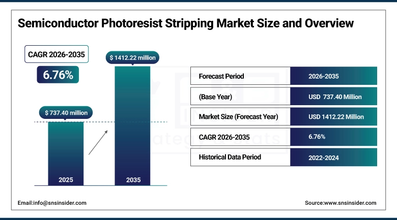
The Semiconductor Photoresist Stripping Market size was valued at USD 737.40 Million in 2025 and is projected to reach USD 1,412.22 Million by 2035, growing at a CAGR of 6.76% during 2026–2035.
Photoresist stripping is a process step carried out after each lithographic patterning and etching cycle in semiconductor manufacturing, removing the photoresist layer from the wafer surface to allow subsequent processing steps to proceed on clean substrate. The step is non-optional in every photolithographic process flow, making it one of the most frequently performed chemical operations in a semiconductor fabrication facility.
Semiconductor Photoresist Stripping Market Size and Forecast:
-
Market Size in 2025: USD 737.40 Million
-
Market Size by 2035: USD 1,412.22 Million
-
CAGR: 6.76% from 2026 to 2035
-
Base Year: 2025
-
Forecast Period: 2026–2035
-
Historical Data: 2022–2024
To Get more information on Semiconductor Photoresist Stripping Market - Request Free Sample Report
Semiconductor Photoresist Stripping Market Trends:
-
Increasing demand for advanced semiconductor nodes (≤7 nm) is driving adoption of high-performance photoresist stripping solutions, with over 60% of leading-edge fabs requiring precision cleaning processes.
-
Growth in EUV lithography is boosting demand for advanced stripping chemistries, as EUV processes account for over 25% of new wafer production capacity in advanced fabs.
-
Rising production of 3D NAND and FinFET devices is increasing process complexity, driving stripping solution usage by 30–40% to ensure residue-free surfaces.
-
Strong focus on yield improvement and defect reduction is accelerating adoption of advanced stripping technologies, reducing defect rates by 20–30% in high-volume manufacturing.
-
Shift toward environmentally friendly and low-damage stripping chemicals is gaining traction, with over 50% of fabs adopting eco-efficient formulations to meet regulatory and sustainability goals.
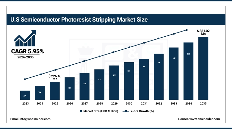
U.S. Semiconductor Photoresist Stripping Market Size Outlook:
The U.S. Semiconductor Photoresist Stripping Market was valued at USD 226.40 Million in 2025 and is projected to reach USD 381.02 Million by 2035, growing at a CAGR of 5.95% during 2026–2035. The United States holds the largest national share within North America, driven by the concentration of advanced semiconductor manufacturing activity at Intel, Micron, Texas Instruments, and GlobalFoundries domestic facilities, alongside a chemical supply industry centered around DuPont, Entegris, and Avantor that provides stripping materials with domestic logistics and technical support advantages
Semiconductor Photoresist Stripping Market Growth Drivers:
-
Wafer Start Volume Expansion Across Foundry and IDM Capacity Additions Translates Directly into Higher Stripping Material and Process Equipment Consumption Across All Node Segments
Photoresist stripping is performed at every lithographic step in semiconductor wafer processing, meaning that the total volume of stripping operations scales with wafer starts rather than with any single application or technology segment. The sustained expansion of semiconductor manufacturing capacity that began during the supply disruptions of 2021 and 2022 and continues through government-backed fab investments in the US, Europe, Japan, and India is creating a multi-year demand floor for stripping materials and equipment that is not dependent on technology transitions alone. TSMC, Samsung, and Intel Foundry capacity additions for advanced node production represent the highest-value portion of this demand growth, as advanced node process flows require more lithographic steps and therefore more stripping operations per wafer than mature node flows.
Semiconductor Photoresist Stripping Market Restraints:
-
Regulatory Restrictions on Legacy Stripping Chemistries and the Process Qualification Costs of Transitioning to Compliant Formulations Create Sustained Cost and Timeline Pressure for Chemical Suppliers and Semiconductor Manufacturers
A substantial portion of the installed base of photoresist stripping processes in semiconductor manufacturing facilities uses chemical formulations that are now subject to tightening environmental and worker safety regulations. N-Methyl-2-pyrrolidone is restricted under REACH regulations in Europe and faces usage limitations in multiple US jurisdictions due to reproductive toxicity concerns, requiring manufacturers to qualify replacement solvents in process flows where NMP-based strippers have been used for decades. Fluorinated solvents subject to broad PFAS restrictions are used in certain specialty stripping applications, and the timeline for their phase-out requires chemical suppliers to develop technically equivalent fluorine-free alternatives and semiconductor manufacturers to run qualification programs that consume engineering resources without adding production capability.
Semiconductor Photoresist Stripping Market Opportunities:
-
Government-Supported Semiconductor Manufacturing Regionalization Creates Multi-Year, Geographically Distributed Demand Growth for Stripping Materials and Process Equipment Across New Fab Installations Outside Established East Asian Manufacturing Concentrations
The CHIPS and Science Act in the United States committed USD 52 billion to domestic semiconductor manufacturing and research, with a significant portion directed toward new fab construction by TSMC Arizona, Samsung Austin, Intel Ohio, and Micron New York. Each of these facilities represents a multi-decade demand anchor for photoresist stripping materials, with procurement relationships established during construction and qualification phases that persist through the operational life of the facility. The European Chips Act targets doubling Europe’s semiconductor production share by 2030, with Intel Magdeburg, TSMC Dresden, and STMicroelectronics Crolles expansions among the investments driving new chemical procurement requirements in geographies where supply chain infrastructure is less developed than in East Asia. Japan’s RAPIDUS project and government support for TSMC Kumamoto and other capacity investments represent equivalent opportunity in a country with existing specialty chemical manufacturing capability.
Semiconductor Photoresist Stripping Market Segment Analysis:
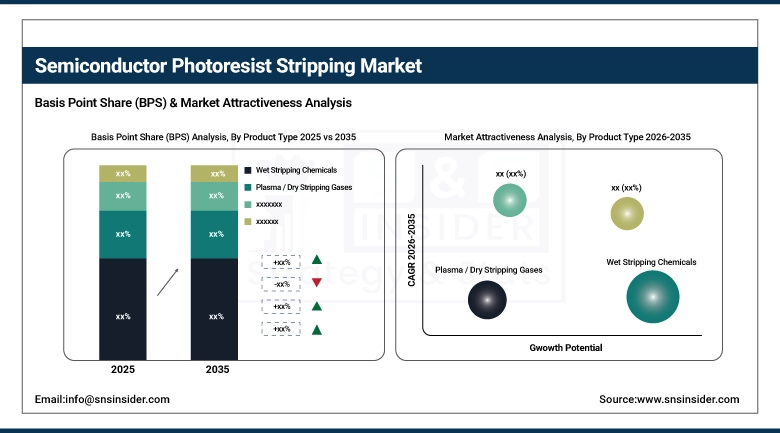
By Product Type: Wet Stripping Chemicals Lead While Solvent-Based Strippers Drive the Fastest Growth Through 2035
Wet Stripping Chemicals dominated with a 38.14% share in 2025, valued at approximately USD 281.24 Million, while Solvent-Based Strippers are expected to grow at the fastest CAGR of approximately 10.03% through 2035.
Wet stripping chemicals hold the leading share across the product type segmentation because they represent the standard process chemistry for bulk photoresist removal across the widest range of semiconductor manufacturing applications. Sulfuric acid and hydrogen peroxide mixtures, commonly referred to as piranha solution, provide highly effective oxidative removal of organic photoresist with well-understood process parameters and are used across front-end and back-end applications at foundries, IDMs, and electronics manufacturers globally. Solvent-based strippers are growing at the fastest rate within the product type segmentation because their superior selectivity and compatibility with resist formulations used in EUV lithography and multi-patterning schemes drives adoption at leading-edge fabs where damage-free removal of complex resist stacks is a process requirement that standard aqueous chemistries cannot always satisfy.
By Application: Front-End Semiconductor Fabrication Leads While LED & Display Manufacturing Drives the Fastest Growth Through 2035
Front-End Semiconductor Fabrication dominated with a 45.27% share in 2025, valued at approximately USD 333.82 Million, while LED & Display Manufacturing is expected to grow at the fastest CAGR of approximately 10.88% through 2035.
Front-end fabrication holds the commanding application share because it encompasses the most lithographic steps in a semiconductor manufacturing process flow and therefore consumes photoresist stripping materials at a higher intensity per wafer than any other application segment. LED and display manufacturing is growing fastest because capacity additions for OLED and microLED display production are creating new photoresist stripping process demand on glass and sapphire substrates at scale, and the rapid adoption of high-resolution displays across consumer electronics, automotive, and commercial display applications is sustaining the capacity investment pace.
By End-User: Semiconductor Foundries Lead While Research & Academic Labs Register Fastest CAGR Through 2035
Semiconductor Foundries dominated with a 36.45% share in 2025, valued at approximately USD 268.78 Million, while Research & Academic Labs are expected to grow at the fastest CAGR of approximately 9.61% through 2035.
Semiconductor foundries represent the largest end-user segment because the pure-play foundry model concentrates wafer production volumes at facilities that are dedicated to manufacturing across a broad range of customers and applications, creating the highest per-facility consumption of photoresist stripping materials. Research and academic laboratories are growing fastest as government investments in semiconductor technology development programs create new process R&D infrastructure at universities and national laboratories, particularly in the United States, Europe, and Japan, where domestic manufacturing initiatives require a corresponding investment in technical education and process development capability.
By Process Node: Mature Nodes (7–28nm) Lead While Advanced Nodes (<7nm) Register Fastest CAGR Through 2035
Mature Nodes (7–28nm) dominated with a 34.21% share in 2025, valued at approximately USD 252.26 Million, while Advanced Nodes (<7nm) are expected to grow at the fastest CAGR of approximately 10.08% through 2035.
Mature nodes hold the largest current share within the process node segmentation because they represent the volume production tier where the greatest number of global wafer starts occur across the widest range of semiconductor product types. Advanced nodes below 7nm are growing fastest because TSMC N3 and N2 ramp, Samsung SF3 and SF2 capacity additions, and Intel 18A production entry are collectively expanding the volume of wafers processed at geometries where the per-wafer stripping chemistry intensity and unit value are higher than at any other node category, creating above-average revenue growth from a smaller but rapidly expanding wafer start base.
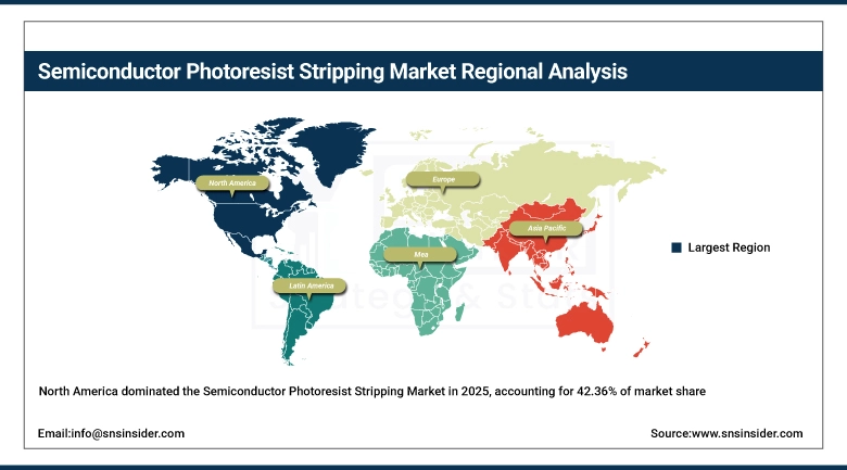
Semiconductor Photoresist Stripping Market Regional Analysis:
North America Semiconductor Photoresist Stripping Market Insights
North America dominated the Semiconductor Photoresist Stripping Market in 2025, accounting for 42.36% of market share, valued at USD 312.36 Million, and is projected to reach USD 549.49 Million by 2035 at a CAGR of 6.48% during the forecast period. North America’s market leadership reflects the combination of an established semiconductor manufacturing base operating across a range of process nodes at Intel, Micron, Texas Instruments, GlobalFoundries, and ON Semiconductor domestic facilities, and a chemical supply infrastructure concentrated in the US that includes global specialty chemical leaders with domestic stripping formulation manufacturing capability.
Get Customized Report as per Your Business Requirement - Enquiry Now
U.S. Semiconductor Photoresist Stripping Market Insights
The United States accounts for 72.48% of North American demand in 2025. The U.S. Semiconductor Photoresist Stripping Market was valued at USD 226.40 Million in 2025 and is projected to reach USD 381.02 Million by 2035, growing at a CAGR of 5.95% during 2026–2035. The US market benefits from co-location of major chemical suppliers, semiconductor equipment manufacturers, and fab operators that enables shorter supply chains, faster technical response, and easier process co-development than is achievable in geographies where these supply chain elements are separated across national boundaries.
Europe Semiconductor Photoresist Stripping Market Insights
Europe held a 22.14% share of the Semiconductor Photoresist Stripping Market in 2025, valued at USD 163.26 Million, and is expected to reach USD 297.70 Million by 2035 at a CAGR of 6.90% during the forecast period. European demand is underpinned by established IDM manufacturing at Infineon Dresden and Munich, STMicroelectronics Crolles and Agrate, NXP Hamburg and Nijmegen, Robert Bosch Reutlingen, and other facilities that collectively represent a substantial base of ongoing wafer production across automotive, industrial, and power semiconductor applications.
Germany Semiconductor Photoresist Stripping Market Insights
Germany leads the European semiconductor photoresist stripping market anchored by Infineon’s Dresden and Munich manufacturing operations, Robert Bosch’s Reutlingen fab producing automotive MEMS and power devices, and the Intel Magdeburg advanced logic fab currently under construction.
Asia Pacific Semiconductor Photoresist Stripping Market Insights
Asia Pacific is expected to grow at the fastest CAGR of approximately 9.17% from 2026 to 2035, rising from USD 210.68 Million in 2025 to USD 463.91 Million by 2035. The region hosts the world’s highest concentration of semiconductor manufacturing capacity, with Taiwan’s TSMC and UMC, South Korea’s Samsung and SK Hynix, Japan’s Kioxia and Renesas, and China’s SMIC and CXMT collectively accounting for the majority of global wafer starts across advanced, mature, and legacy process nodes. Asia Pacific’s above-average growth rate reflects both the continued expansion of existing manufacturing capacity in Taiwan, South Korea, and Japan and the accelerating pace of Chinese domestic capacity addition across a range of nodes as semiconductor self-sufficiency investment intensifies.
China Semiconductor Photoresist Stripping Market Insights
China is the dominant growth contributor within Asia Pacific for photoresist stripping market expansion, driven by government-mandated domestic semiconductor capacity investment across SMIC, CXMT, Yangtze Memory Technologies, and numerous smaller fabs that are adding wafer starts at mature and legacy nodes where domestic supply chain development is most advanced.
Latin America and Middle East & Africa Semiconductor Photoresist Stripping Market Insights
Latin America held approximately 4.89% of the global Semiconductor Photoresist Stripping Market in 2025, valued at USD 36.06 Million, and is expected to reach USD 75.84 Million by 2035 at a CAGR of 8.61% during the forecast period. Brazil and Mexico represent the primary markets, supported by electronics assembly operations and a growing semiconductor packaging presence in Mexico’s manufacturing corridor that creates back-end stripping chemistry demand. Middle East & Africa held approximately 2.04% of market share in 2025, valued at USD 15.04 Million, and is expected to reach USD 25.28 Million by 2035 at a CAGR of 5.94% during the forecast period.
Competitive Landscape for Semiconductor Photoresist Stripping Market:
DuPont
DuPont’s semiconductor solutions segment supplies wet stripping chemistries, edge bead removers, and surface preparation materials to semiconductor manufacturers across the full range of process node categories. The company’s history in semiconductor materials chemistry provides application knowledge depth that underpins formulation development for EUV-compatible and advanced node process requirements.
In January 2025, DuPont announced a supply agreement with a major US foundry for photoresist stripping and surface preparation chemistry supply to a new fab facility under construction in Arizona, with long-term pricing and supply security terms structured to support the fab’s multi-decade operational horizon.
Entegris
Entegris approaches the stripping market with an integrated materials purity platform that combines stripping chemistry supply with the filtration, storage, and dispensing systems required to maintain the chemical consistency that advanced node manufacturing demands.
In March 2025, Entegris expanded its Kulim, Malaysia manufacturing facility to increase production capacity for semiconductor process chemicals including photoresist strippers serving Asia Pacific foundry and IDM customers, with the expansion scheduled for qualification completion ahead of projected regional demand increases from new fab startups.
Semiconductor Photoresist Stripping Companies are:
-
DuPont
-
Merck KGaA
-
Fujifilm
-
Tokyo Ohka Kogyo
-
Mitsubishi Gas Chemical
-
Kanto Chemical
-
Avantor
-
Solexir
-
Anji Microelectronics
-
JSR Corporation
-
Dow Inc.
-
Shin-Etsu Chemical
-
Sumitomo Chemical
-
Applied Materials
-
Advanced Energy Industries
-
Brewer Science
-
Lam Research
-
Screen Holdings Co., Ltd.
| Report Attributes | Details |
|---|---|
| Market Size in 2025 | USD 737.40 Million |
| Market Size by 2035 | USD 1412.22 Million |
| CAGR | CAGR of 6.76% From 2026 to 2035 |
| Base Year | 2025 |
| Forecast Period | 2026-2035 |
| Historical Data | 2022-2024 |
| Report Scope & Coverage | Market Size, Segments Analysis, Competitive Landscape, Regional Analysis, DROC & SWOT Analysis, Forecast Outlook |
| Key Segments | • By Product Type (Wet Stripping Chemicals, Plasma / Dry Stripping Gases, Solvent-Based Strippers, and Thermal Stripping Materials) • By Application (Front-End Semiconductor Fabrication, Back-End Packaging & Assembly, MEMS & Sensors, and LED & Display Manufacturing) • By End-User (Semiconductor Foundries, Integrated Device Manufacturers (IDMs), Electronics & Consumer Device Companies, and Research & Academic Labs) • By Process Node / Technology (Advanced Nodes (<7nm), Mature Nodes (7–28nm), Legacy Nodes (>28nm), and Emerging Technologies (3D ICs, Heterogeneous Integration)) |
| Regional Analysis/Coverage | North America (US, Canada), Europe (Germany, UK, France, Italy, Spain, Russia, Poland, Rest of Europe), Asia Pacific (China, India, Japan, South Korea, Australia, ASEAN Countries, Rest of Asia Pacific), Middle East & Africa (UAE, Saudi Arabia, Qatar, South Africa, Rest of Middle East & Africa), Latin America (Brazil, Argentina, Mexico, Colombia, Rest of Latin America). |
| Company Profiles | DuPont, Entegris, Merck KGaA, Fujifilm, Tokyo Ohka Kogyo, Mitsubishi Gas Chemical, Kanto Chemical, Avantor, Technic Inc., Solexir, Anji Microelectronics, JSR Corporation, Dow Inc., Shin‑Etsu Chemical, Sumitomo Chemical, Applied Materials, Advanced Energy Industries, Brewer Science, Lam Research, Screen Holdings Co., Ltd. |
Get in Touch
