Semi-insulating Silicon Carbide Wafer market Size:
Get more information on Semi-insulating silicon carbide wafer Market - Request Free Sample Report
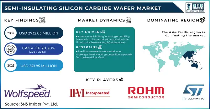
The Semi-Insulating Silicon Carbide Wafer Market Size was valued at USD 521.85 million in 2023 and is expected to grow to USD 2732.83 million by 2032 and grow at a CAGR Of 20.20 % over the forecast period of 2024-2032.
The semi-insulating silicon carbide (SiC) wafer market is experiencing significant growth, driven by the rising demand for power electronics in industries such as automotive, renewable energy, and industrial automation. SiC wafers are crucial for power-efficient devices, offering superior electrical properties, high thermal conductivity, and the ability to withstand higher voltages and temperatures compared to traditional silicon. This makes SiC an ideal material for electric vehicle (EV) applications, where it enhances power system performance, including inverters, motors, and battery management systems. With the growing global preference for electric vehicles (EVs), SiC adoption in battery electric vehicles (BEVs) is projected to increase substantially. over 50% of BEVs could rely on SiC powertrains, up from about 30% today, as automakers transition to SiC-based systems for better efficiency, longer range, and faster charging times. This shift will accelerate SiC demand, with the market set to benefit from the widespread adoption of 800-volt BEV systems. challenges such as high defect rates and yield losses complicate supply estimates. Despite this, SiC wafer providers are increasing production capacity, with plans to ramp up 150-mm SiC wafer production from 2.8 million in 2023 to 10.9 million, a more than threefold increase. Moreover, the industry is exploring 200-mm wafer capabilities, which, while more difficult to manufacture, offer long-term cost advantages. As companies master the 200-mm process, the cost per square mm will decrease, providing a competitive edge in the market. These advancements ensure that the SiC wafer market will continue to expand, driven by increasing demand in BEVs, renewable energy, and industrial automation.
Semi-Insulating Silicon Carbide Wafer Market Dynamics
Drivers
-
Advancements in Slicing Technologies and Rising Demand from 5G and Industrial Automation Drive Growth in the Semi-Insulating SiC Wafer Market
The semi-insulating silicon carbide (SiC) wafer market is experiencing robust growth driven by the increasing adoption of industrial automation, robotics, and 5G communication technologies. SiC wafers, known for their ability to handle high voltages and temperatures, are essential in powering high-performance robots and automation systems used in manufacturing and logistics. Their superior thermal conductivity and efficiency ensure optimal performance and heat dissipation in these systems. In parallel, the rise of 5G technology is creating significant demand for SiC wafers in high-frequency power semiconductors used in 5G base stations and communication equipment. The use of advanced slicing technologies, such as multi-wire slurry sawing and diamond wire sawing, is accelerating SiC wafer production, with laser slicing emerging as a more efficient method. Studies have shown that laser slicing is 92% more efficient than wire sawing, with half the material loss, making it a preferred choice for wafer slicing. Laser slicing cuts wafers using modified layers parallel to the laser propagation direction, while wire sawing involves modified layers perpendicular to the laser propagation direction to dice wafers. With companies like ON Semiconductor expanding SiC production capabilities, the market is poised for continued growth as SiC wafers play a pivotal role in enabling the next generation of industrial automation, 5G infrastructure, and robotics, positioning SiC as a critical material in shaping future technological advancements.
Restraints
-
The silicon-insulated wafer market faces challenges from increasing competition, especially from gallium nitride (GaN).
While silicon carbide (SiC) wafers offer high thermal conductivity and exceptional performance in high-voltage applications, GaN is increasingly being adopted for power electronics and radio frequency (RF) applications due to its comparable advantages, such as higher electron mobility, lower power consumption, and the ability to operate at higher temperatures. The shift towards GaN in industries such as telecommunications, automotive, and power systems poses a considerable threat to the SiC wafer market. GaN's lower manufacturing costs and smaller form factor make it an attractive alternative, especially for smaller-scale power applications and RF components, where SiC wafers are traditionally used. Moreover, GaN’s potential to support next-generation technologies like 5G communications and electric vehicles (EVs) has prompted its adoption in these rapidly growing sectors. This competition is compounded by the ongoing innovation in GaN manufacturing techniques, which are driving efficiency improvements and reducing production costs, further eroding SiC’s competitive edge. Additionally, GaN is more suited to smaller geometries, enhancing its appeal for power-efficient applications in consumer electronics, further limiting the growth opportunities for SiC wafers. As the adoption of GaN technology expands, it could hinder the growth of the SiC wafer market, particularly in lower-voltage and medium-power applications, where SiC is not always the most cost-effective option. Consequently, the increasing shift toward GaN-based solutions could significantly impact SiC wafer demand, slowing the market’s potential growth.
Semi-Insulating Silicon Carbide Wafer Market Segment Analysis
By Type
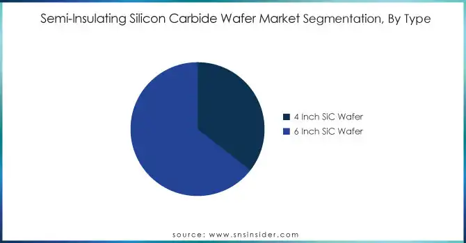
The 6-inch SiC wafer segment dominated the semi-insulating silicon carbide wafer market in 2023, accounting for approximately 65% of the total market share. This dominance is driven by the 6-inch wafer's ideal size for a range of power semiconductor applications, particularly in electric vehicles (EVs), power electronics, and telecommunications. The 6-inch wafer size strikes a balance between cost-effectiveness, performance, and manufacturing scalability, making it highly favored by semiconductor manufacturers. As industries increasingly adopt SiC-based components for high-voltage, high-frequency applications, the demand for 6-inch wafers continues to grow. Additionally, the ability to optimize the wafer's performance for specific power applications in automotive and energy sectors further bolsters its market share. With the rise of EVs and 5G technologies, the 6-inch SiC wafer segment is expected to maintain its strong market position.
By Application
The power device segment dominated the semi-insulating silicon carbide (SiC) wafer market in 2023, accounting for approximately 41% of the total market share. This is largely due to SiC’s exceptional performance in high-power and high-efficiency applications, where it offers superior thermal conductivity, low power loss, and high voltage tolerance. SiC wafers are crucial in power devices used in electric vehicles (EVs), renewable energy systems, industrial equipment, and power electronics. As the demand for energy-efficient solutions grows, especially with the rise of EVs and renewable energy projects, SiC-based power devices are becoming increasingly popular. Their ability to operate at higher temperatures and voltages makes them an ideal choice for these applications, driving significant growth in the power device segment. This trend is expected to continue, further strengthening the dominance of the power device segment in the market.
Semi-Insulating Silicon Carbide Wafer Market Regional Outlook
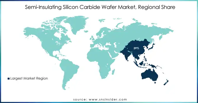
In 2023, the Asia-Pacific region dominated the semi-insulating silicon carbide (SiC) wafer market, accounting for approximately 39% of the total market share. The region's dominance is driven by the rapid industrialization and technological advancements in key countries like China, Japan, South Korea, and India. China, with its large-scale manufacturing base and government policies supporting green technologies, is a major driver of demand for SiC wafers, particularly in electric vehicles (EVs) and renewable energy sectors. Japan and South Korea are home to leading SiC wafer manufacturers, which contribute significantly to the development of high-performance power devices used in industrial automation, telecommunications, and automotive applications. Additionally, India’s push towards electrification and energy-efficient solutions further bolsters SiC wafer adoption. These countries' investments in renewable energy, EV infrastructure, and advanced semiconductor manufacturing technologies make Asia-Pacific the dominant region for SiC wafers. The region's ongoing advancements in power electronics, coupled with its supportive government initiatives and technological innovation, are expected to maintain its leadership in the SiC wafer market, positioning Asia-Pacific as the global hub for SiC wafer production and application development.
North America is expected to be the fastest-growing region in the semi-insulating silicon carbide (SiC) wafer market from 2024 to 2032. Key drivers include the rising demand for SiC-based power devices across automotive, telecommunications, renewable energy, and industrial automation sectors. The adoption of electric vehicles (EVs) is a major factor, with SiC wafers improving EV powertrain and charging system efficiency. Additionally, North America's shift towards renewable energy and energy-efficient solutions further boosts the demand for SiC wafers in high-voltage, high-temperature, and high-frequency applications. The region’s strong semiconductor manufacturing presence, with companies like Wolfspeed and Infineon investing in SiC technology, further accelerates market growth. Government support for strengthening the domestic semiconductor supply chain also fuels market expansion, positioning North America as a key player in the SiC wafer market.
Need any customization research on Semi-insulating silicon carbide wafer Market - Enquiry Now
Key Players:
Some of the Major Players in Semi-Insulating Silicon Carbide Wafer Market along with their product:
-
WOLFSPEED, INC. (4-Inch and 6-Inch SiC Wafers, Power Devices, RF Devices)
-
II-VI Incorporated (Semi-Insulating and Conductive SiC Substrates, Power Electronics)
-
STMicroelectronics (SiC Power Devices, Automotive Modules)
-
ROHM CO., LTD (SiC Schottky Diodes, SiC MOSFETs, SiC Wafers)
-
SHOWA DENKO K.K. (High-Purity SiC Wafers, Power Semiconductor Substrates)
-
SICC Co., Ltd. (SiC Wafers, Optoelectronics Substrates)
-
SK siltron Co. Ltd. (Conductive and Semi-Insulating SiC Wafers)
-
TankeBlue CO., LTD. (SiC Substrates, Epitaxial Wafers)
-
CETC Solar Energy Holdings Co., Ltd. (High-Purity SiC Wafers, Solar and Semiconductor Substrates)
-
Synlight (SiC Wafers for Optoelectronics and Power Devices)
-
Norstel AB (High-Quality SiC Wafers, Epitaxial Layers)
-
Cree Inc. (SiC Power Modules, 4-Inch and 6-Inch SiC Wafers)
-
GeneSiC Semiconductor Inc. (SiC Diodes, MOSFETs)
-
Infineon Technologies AG (SiC Power Electronics, Automotive SiC Solutions)
-
Hitachi Power Semiconductor Device Ltd. (SiC Modules for Power Systems)
-
San’an Optoelectronics Co., Ltd. (SiC Wafers for Optoelectronics and LEDs)
-
GlobalWafers Co., Ltd. (Semi-Insulating SiC Wafers, Epitaxial Wafers)
-
PVA TePla AG (SiC Wafer Manufacturing Equipment, Inspection Systems)
-
Advanced Micro Devices, Inc. (SiC Power Devices)
-
LPE Spa (Epitaxial SiC Wafer Processing Systems)
-
Okmetic Oy (High-Purity SiC Wafers for Industrial Applications)
-
Kyocera Corporation (SiC Components and Substrates)
-
Mitsubishi Electric Corporation (SiC Power Modules, Industrial Solutions)
-
ABB Ltd. (SiC Semiconductor Solutions for Renewable Energy)
-
Panasonic Corporation (SiC Power Devices, Automotive Applications)
-
Dow Corning (SiC Wafers, Thermal Management Solutions)
-
Tokuyama Corporation (High-Purity SiC Materials for Wafers)
-
Saint-Gobain (SiC Substrates, Advanced Materials)
-
Sumitomo Electric Industries, Ltd. (SiC Power Semiconductor Substrates)
-
AGC Inc. (High-Purity SiC Wafers for Power Electronics)
List of Some companies that are potential customers and suppliers for the semi-insulating silicon carbide (SiC) wafer market:
Potential Customers:
Automotive Manufacturers
-
Tesla
-
General Motors
-
Ford
-
Toyota
-
BMW
Telecommunications Companies
-
Verizon
-
AT&T
-
T-Mobile
-
Qualcomm
Renewable Energy Companies
-
SunPower
-
First Solar
-
Siemens Gamesa
Industrial Automation Companies
-
ABB
-
Siemens
-
Rockwell Automation
-
Schneider Electric
Semiconductor Companies
-
Intel
-
NVIDIA
-
Texas Instruments
-
Broadcom
Power Electronics Companies
-
Mitsubishi Electric
-
Infineon Technologies
-
ON Semiconductor
-
Vishay Intertechnology
Aerospace and Defense Companies
-
Lockheed Martin
-
Northrop Grumman
-
Raytheon Technologies
-
Boeing
Energy Storage Companies
-
Panasonic
-
LG Chem
-
BYD
Recent Development
-
April 2024 – ROHM Group's SiCrystal and STMicroelectronics have expanded their existing silicon carbide (SiC) wafer supply agreement. The new multi-year deal, valued at USD 230 million, will increase the supply of 150mm SiC substrate wafers to support STMicroelectronics' ramp-up of manufacturing for automotive and industrial customers worldwide.
-
October 2024 – Infineon Technologies has unveiled the world’s thinnest silicon power wafer, measuring just 20 micrometers thick, a quarter of the thickness of a human hair. This breakthrough enables high-scale processing and handling of ultra-thin 300mm wafers, setting a new standard in semiconductor manufacturing.
-
May 2024 – Saint-Gobain Performance Ceramics & Refractories has highlighted the increasing importance of silicon carbide rods in high-temperature industrial applications. These rods, renowned for their wear resistance, low thermal expansion, and high thermal conductivity, are crucial in furnace operations, ensuring extended service life and reducing downtime for optimal return on investment.
| Report Attributes | Details |
| Market Size in 2023 | USD 521.85 Million |
| Market Size by 2032 | USD 2732.83 Million |
| CAGR | CAGR of 20.20% From 2024 to 2032 |
| Base Year | 2023 |
| Forecast Period | 2024-2032 |
| Historical Data | 2020-2022 |
| Report Scope & Coverage | Market Size, Segments Analysis, Competitive Landscape, Regional Analysis, DROC & SWOT Analysis, Forecast Outlook |
| Key Segments | • By Type (4-inch SiC Wafer, 6-inch SiC Wafer) • By Application (Power Devices, Electronics, and Optoelectronics, Wireless Infrastructure, and Others) |
| Regional Analysis/Coverage | North America (US, Canada, Mexico), Europe (Eastern Europe [Poland, Romania, Hungary, Turkey, Rest of Eastern Europe] Western Europe] Germany, France, UK, Italy, Spain, Netherlands, Switzerland, Austria, Rest of Western Europe]), Asia Pacific (China, India, Japan, South Korea, Vietnam, Singapore, Australia, Rest of Asia Pacific), Middle East & Africa (Middle East [UAE, Egypt, Saudi Arabia, Qatar, Rest of Middle East], Africa [Nigeria, South Africa, Rest of Africa], Latin America (Brazil, Argentina, Colombia, Rest of Latin America) |
| Company Profiles | Wolfspeed, II-VI Incorporated, STMicroelectronics, ROHM CO., LTD, Showa Denko K.K., SICC Co., Ltd., SK Siltron Co. Ltd., TankeBlue CO., LTD., CETC Solar Energy Holdings Co., Ltd., Synlight, Norstel AB, Cree Inc., GeneSiC Semiconductor Inc., Infineon Technologies AG, Hitachi Power Semiconductor Device Ltd., San'an Optoelectronics Co., Ltd., GlobalWafers Co., Ltd., PVA TePla AG, Advanced Micro Devices, Inc., LPE Spa, Okmetic Oy, Kyocera Corporation, Mitsubishi Electric Corporation, ABB Ltd., Panasonic Corporation, Dow Corning, Tokuyama Corporation, Saint-Gobain, Sumitomo Electric Industries, Ltd., and AGC Inc. are key players in the SiC wafer and power device sector. |
| Key Drivers | • Advancements in Slicing Technologies and Rising Demand from 5G and Industrial Automation Drive Growth in the Semi-Insulating SiC Wafer Market. |
| Restraints | • The silicon-insulated wafer market faces challenges from increasing competition, especially from gallium nitride (GaN). |
Get in Touch
