
Thin Wafer Processing and Dicing Equipment Market Report Scope and Overview:
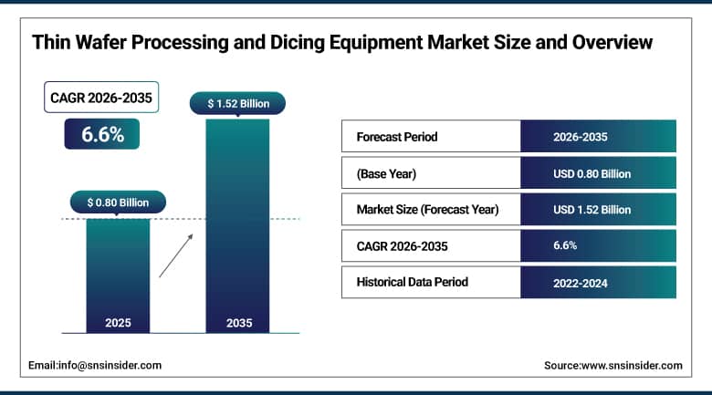
The Thin Wafer Processing and Dicing Equipment Market size was valued at USD 0.80 Billion in 2025 and is projected to reach USD 1.52 Billion by 2035, registering a CAGR of 6.6% from 2026 to 2035.
Thin Wafer Processing and Dicing Equipment Market is extremely important for advanced semiconductor fabrication since this market provides thin wafer processing and singulation required for 3D-IC packaging, power devices, and memory stacking. The market is fueled by rapid expansion in through-silicon-via memory and logic integration, increased use of silicon carbide and gallium nitride power devices in electric vehicles, further miniaturization of consumer electronics demanding stricter wafer thinness, and wider implementation of plasma and stealth dicing of ultra-thin wafers. Rapid expansion can be observed in thickness feedback solutions powered by AI, laser singulation, and pilot lines of 3D-IC supported by government funding, as foundries, OSATs, and equipment makers are making heavy investments in wafer handling technologies maintaining yield at sub-50 micron thicknesses.
In June 2026, Applied Materials introduced its Producer Avila 2 PECVD system, aimed at improving mechanical stability for ultra-thin DRAM dies used in HBM stacking by depositing stress-balanced dielectric films that reduce warpage risk during aggressive wafer thinning.
To Get More Information On Thin Wafer Processing and Dicing Equipment Market - Request Free Sample Report
Thin Wafer Processing and Dicing Equipment Market Trends
-
Rising adoption of TSV memory and logic integration is accelerating demand for sub-50-micron wafer-thinning equipment.
-
Growing silicon-carbide and gallium-nitride power-device adoption in EVs is widening plasma and laser dicing demand.
-
Increasing consumer-electronics miniaturization continues tightening wafer-thickness tolerances and driving equipment upgrades.
-
Advancing AI-driven thickness-feedback and stress-compensation systems are improving yield at ultra-thin dimensions.
-
Expanding government-funded 3D-IC pilot lines in China and the EU continue reinforcing equipment capital spending.
U.S. Thin Wafer Processing and Dicing Equipment Market Size Outlook
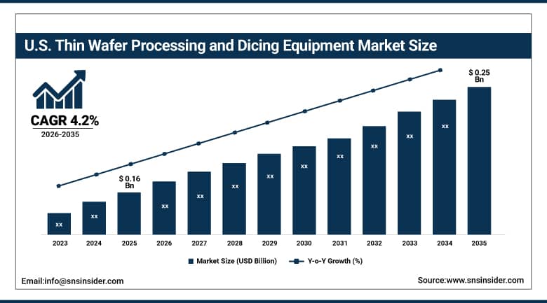
The U.S. Thin Wafer Processing and Dicing Equipment Market was valued at approximately USD 0.16 Billion in 2025 and is projected to reach approximately USD 0.25 Billion by 2035, registering a CAGR of approximately 4.2% from 2026 to 2035.
Demand across the United States continued to be shaped by increasing semiconductor content in electric vehicles and consumer electronics, boosting demand for thinning, dicing, and handling equipment supporting power devices, sensors, and control integrated circuits. Foundry expansions linked to domestic industrial-policy incentives required parity with Asian process performance, including the importation of advanced chemical-mechanical-polishing, carrier-bond, and plasma-dicing technologies. Environmental, health, and safety regulations continued pushing fabs toward low-particulate plasma tools over blade systems, while large capital commitments by multinational integrated device manufacturers shortened payback periods for equipment vendors and diversified geographic revenue streams across the United States through the forecast period.
In May 2024, Lam Research Corporation unveiled its plan of expanding its supply chain for manufacturing equipment for semiconductors in India, with a focus on precision components and gas delivery equipment for wafer thinning, but without any resistance to government incentives for local manufacturing.
Thin Wafer Processing and Dicing Equipment Market Segment Analysis
-
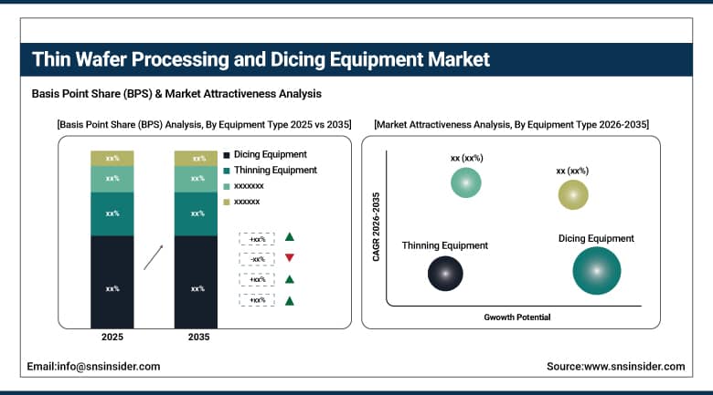
By Equipment Type, the Dicing Equipment segment dominated the Thin Wafer Processing and Dicing Equipment Market with approximately 62.00% share in 2025, while the Thinning Equipment segment is the fastest growing with a CAGR of approximately 7.50%.
-
By Application, the Memory and Logic (TSV) segment dominated the Thin Wafer Processing and Dicing Equipment Market with approximately 31.00% share in 2025, while the Power Devices segment is the fastest growing with a CAGR of approximately 8.40%.
-
By End-Use Industry, the Consumer Electronics segment dominated the Thin Wafer Processing and Dicing Equipment Market with approximately 41.50% share in 2025, while the Automotive segment is the fastest growing with a CAGR of approximately 8.50%.
By Equipment Type: Dicing Equipment Leads, Thinning Equipment Grows Fastest
Dicing Equipment held the lead in the Thin Wafer Processing and Dicing Equipment Market in 2025 due to the critical need for die separation regardless of the process node type whether legacy or advanced. Blade technologies remain dominant in consumer IC applications where mature cost-per-cut metrics prevail; yet plasma and stealth technologies witness increasing adoption with the growing preference for wafer-level packages where blade-based microcracks cannot be tolerated. Wafers intended for advanced 3D integration are commonly subject to back-grinding at ultra-thin thicknesses and subsequent plasma dicing, which entails a substantially higher requirement for equipment on a per-wafer basis than the conventional blade technology.
Thinning Equipment is registering the fastest growth in the Thin Wafer Processing and Dicing Equipment Market, as semiconductor manufacturers strive for more compact, ultra-thin wafers and high-performance devices across memory, power, and advanced-packaging applications. Recent improvements in precision grinding and chemical-mechanical polishing are resulting in higher yields, reduced wafer stress, and improved compatibility with fragile substrates, benefiting high-density memory and power-device manufacturers specifically. Integrated metrology, vibration-free stages, and AI-driven thickness-feedback loops collectively raise average selling prices, so the segment already commands a greater revenue-per-unit ratio within the market. Continued transition toward sub-50-micron wafer stacks keeps this segment's growth well above the broader market average through 2035.
By Application: Memory and Logic (TSV) Leads, Power Devices Grow Fastest
Memory and Logic (TSV) dominated the Thin Wafer Processing and Dicing Equipment Market in 2025 due to the immediate three-dimensional stacking benefits within high-bandwidth-memory modules used in AI server accelerators. Chipmakers are moving toward vertical integration to bypass the limits of planar scaling, with TSV-stacked DRAM and chiplet-based CPUs requiring wafers thinned to extreme thinness that traditional double-side grind systems cannot process without inducing warpage. Leading foundries have earmarked substantial budgets for advanced logic ramps that include large batches of carrier-debond, laser-debond, and plasma-dicing tools, amplifying throughput requirements across high-volume fabs. Equipment suppliers offering integrated metrology and real-time stress compensation continue gaining share, keeping Memory and Logic the largest application category through the forecast period.
Power Devices are registering the fastest growth in the Thin Wafer Processing and Dicing Equipment Market, fueled by traction inverters, onboard chargers, and renewables-linked power conversion that depend on wide-bandgap silicon-carbide and gallium-nitride devices. These materials require ultra-clean kerf edges and present higher hardness than conventional silicon, aligning closely with plasma and stealth dicing value propositions that minimize chipping and contamination. As electric-vehicle unit shipments increase, tool demand intensifies far beyond proportional wafer counts, because compound-semiconductor substrates typically break more blades and must transition to laser or plasma singulation earlier in the process. Automotive qualification regimes requiring multi-site redundancy continue increasing equipment installations, sustaining this segment's above-average growth trajectory through 2035.
By End-Use Industry: Consumer Electronics Leads, Automotive Grows Fastest
Consumer Electronics was the dominant end-user segment within the Thin Wafer Processing and Dicing Equipment Market in 2025 due to the growing demand for thinner and more lightweight semiconductors with superior performance because of the increasing use of smartphones, tablets, and wearables. The increased precision cutting and wafer dicing required for the manufacture of these small electronic devices will further drive the usage of automated machines and lasers, along with AI-based quality assurance systems that speed up the process of processing. Smartphone manufacturing volumes include the use of thin wafers in application processors and memory interfaces, where leading device manufacturers dictate their specifications across their entire range of products.
Automotive is witnessing the fastest growth across end use markets, especially the rise in electric cars and self-driving cars, which are boosting the wafer-level demand for power devices, sensors and control ICs. Key trends here include the availability of strong handling technologies for large, thin wafers, high precision dicing and the inclusion of automated inspection technology in order to achieve reliability and yield in critical applications. The increase in semiconductor content per car due to the advent of advanced driver-assisted systems and battery management electronics further increases the addressable market for thin wafer processing equipment beyond the existing consumer application.
Regional Analysis
|
Region |
Major Country |
Share within Region, 2025 (%) |
|
North America |
United States |
89.00% |
|
Europe |
Germany |
38.00% |
|
Asia Pacific |
Taiwan |
36.00% |
|
Middle East and Africa |
South Africa |
30.00% |
|
Latin America |
Brazil |
45.00% |
Asia Pacific Thin Wafer Processing and Dicing Equipment Market Insights
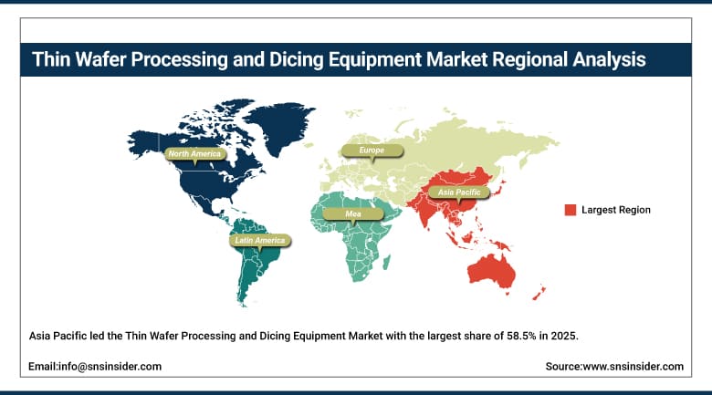
Asia Pacific led the Thin Wafer Processing and Dicing Equipment Market with the largest share of 58.5% in 2025 and is also advancing at the fastest pace among all regions, registering a CAGR of 8.3% through 2035. The region's dual leadership stems from Taiwan's foundry leadership, South Korea's memory output, and China's subsidy-backed capacity buildout, supported by a wave of fab announcements requiring intensive thin-wafer processing. Japanese equipment makers supply a majority of blade and stealth dicing systems regionally, ensuring vendor proximity and after-sales service density that reinforce Asia Pacific's dominant position throughout the forecast period.
Taiwan accounted for roughly 36.00% of regional revenue, anchored by its position as home to leading semiconductor foundries requiring continuous thin-wafer processing capacity. China's rapid semiconductor fabrication expansion and advanced-packaging initiatives, supported by government policies encouraging chip self-sufficiency, added substantial additional demand, while South Korea and Japan contributed further momentum through memory-device manufacturing and precision equipment supply. That combination of foundry scale and genuine memory and power-device demand kept Asia Pacific the largest and fastest-growing Thin Wafer Processing and Dicing Equipment market through the forecast period.
Get Customized Report as Per Your Business Requirement - Enquiry Now
North America Thin Wafer Processing and Dicing Equipment Market Insights
North America held a substantial share of global Thin Wafer Processing and Dicing Equipment Market revenue in 2025, supported by increasing adoption of cutting-edge semiconductor manufacturing technologies driven by demand from consumer electronics, automotive, and high-performance-computing industries. Foundry expansions linked to domestic industrial-policy incentives required parity with Asian process performance, including the importation of advanced chemical-mechanical-polishing, carrier-bond, and plasma-dicing technologies. Investments in automation, laser dicing, and ultra-thin wafer processing continued accelerating to support growing domestic demand for automated semiconductor fabrication.
The United States accounted for roughly 89.00% of regional revenue, anchored by increasing semiconductor content in electric vehicles and consumer electronics driving demand for thinning, dicing, and handling equipment supporting power devices, sensors, and control integrated circuits. Canada contributed further regional demand through automotive and industrial-automation applications, and that combined strength kept North America a critical Thin Wafer Processing and Dicing Equipment market through the forecast period.
Europe Thin Wafer Processing and Dicing Equipment Market Insights
Europe held a meaningful share of global Thin Wafer Processing and Dicing Equipment Market revenue, growing steadily as demand for advanced packaging and high-performance semiconductor devices increased across the automotive, consumer-electronics, and industrial-automation sectors. Manufacturers deployed laser and plasma dicing technologies, ultra-thin wafer-handling systems, and AI-based process monitoring to improve efficiency and yield, with government support for advanced electronics and semiconductor fabrication research continuing to stimulate regional market development.
Germany led demand at roughly 38.00% of European revenue, positively impacted by strong automotive and consumer-electronics markets requiring electric vehicles, efficient computing, and industrial-automation technologies. The United Kingdom and France contributed further regional demand through automotive-manufacturing and industrial applications, keeping European demand for Thin Wafer Processing and Dicing Equipment technology on a steady upward trajectory through the forecast period.
Latin America and Middle East & Africa Thin Wafer Processing and Dicing Equipment Market Insights
Latin America and the Middle East and Africa both showed steady growth, driven by expanding automotive-electronics assembly, consumer-electronics manufacturing, and industrial-automation initiatives across both regions. Rising domestic assembly and semiconductor-import initiatives continued generating demand for laser dicing, wafer thinning, and automated-handling solutions that provide precise processing for fragile and thin components throughout the forecast period.
South Africa led Middle East and Africa demand at roughly 30.00% of regional revenue, supported by industrial automation, automotive electronics, and consumer-electronics manufacturing driving gradual adoption of ultra-thin wafer-processing technologies. In Latin America, Brazil accounted for the largest share of regional revenue at roughly 45.00%, with expanding automotive-electronics and industrial-automation investment continuing to anchor regional demand for Thin Wafer Processing and Dicing Equipment technology through the forecast period.
Market Dynamics
Growth Drivers: 3D-IC Integration and Automotive Power-Device Demand
The industry is driven by chipmakers moving toward vertical integration to bypass the limits of planar scaling, with TSV-stacked DRAM and chiplet-based CPUs requiring wafers thinned to extreme thinness that traditional double-side grind systems cannot process without inducing warpage. Leading foundries have earmarked multi-billion-dollar budgets for advanced logic ramps that include large batches of carrier-debond, laser-debond, and plasma-dicing tools, amplifying throughput requirements as single fabs consume tens of thousands of wafers monthly, each requiring ultra-clean singulation to protect sensitive interconnect structures.
Rising adoption of RFID, smart cards, and automotive power integrated circuits further reinforces this driver, as contactless payment cards and vehicle electrification require dies with reduced thicknesses for radio-frequency efficiency and thermal performance. Silicon-carbide traction inverters in battery-electric vehicles rely on ultra-thin wafers to reduce thermal resistance, driving demand for advanced grinding, chemical-mechanical-polishing, and stress-relief modules, and that combination of 3D-IC integration and automotive electrification is exactly what keeps demand climbing at such a sustained pace.
Restraints: Wafer Warpage and High Equipment Costs
Reducing wafer thickness magnifies internal stress gradients and accentuates post-grind bow, with yield losses from die cracking reaching meaningful levels in aggressive TSV stacks. Bow-corrective carriers and chuck-level active compensation add cost and complexity yet remain essential, while plasma-based singulation introduces localized heating that can worsen warp if chuck cooling is inadequate, necessitating closed-loop thermal management that adds further engineering overhead.
A complete line integrating grind, chemical-mechanical polishing, temporary bond-debond, stealth or plasma dicing, and inline metrology can exceed tens of millions of dollars, a threshold unattainable for many specialty integrated-device manufacturers. Tier-two fabs often outsource to service providers, relinquishing control over their schedules, while financing challenges lengthen sales cycles and concentrate purchasing power among vendors able to bundle tools, service, and leasing packages, constraining the addressable customer pool across the market.
Opportunities: Sub-50-Micron Processing and Advanced-Packaging Expansion
White space is forming around sub-50-micron wafer flows that combine thinning, stress management, and singulation into repeatable, high-yield process modules, particularly where blade dicing faces chipping and microcrack limits. Integration of artificial intelligence and automation in wafer handling continues improving yield, efficiency, and process reliability, accelerating equipment adoption in high-volume manufacturing settings across memory, power, and advanced-packaging applications.
Tying thin-die integrity requirements in advanced packaging to equipment upgrades across regions offers a second substantial opportunity, as capacity-expansion announcements explicitly linking investment to advanced packaging and silicon photonics raise the need for thin-wafer handling and precision singulation at packaging-centric fabs. Expanding electric-vehicle production and 5G deployment continue widening the addressable base for high-throughput thinning and dicing lines, positioning suppliers with proven, scalable technology to capture meaningful share through the forecast period.
Recent Developments:
-
2026: ACCRETECH (Tokyo Seimitsu) announced a major product-line upgrade and strategic capacity expansion for laser dicers and grinders in China, targeting higher-throughput wafer processing.
-
2026: TRUMPF partnered with LIDROTEC, announced at Semicon Korea, to move liquid-assisted laser dicing toward mass production for fragile and compound-material wafers.
-
2024: DISCO disclosed a major capacity expansion program of USD 275 million to strengthen production for high-accuracy dicing equipment supporting plasma, stealth, and laser singulation.
-
2024: MKS Instruments unveiled plans to establish its first Asian factory in Penang, Malaysia, dedicated to thin wafer processing and dicing equipment production.
Thin Wafer Processing and Dicing Equipment Companies are:
-
Disco Corporation
-
Tokyo Seimitsu Co., Ltd. (ACCRETECH)
-
ASMPT
-
Advanced Dicing Technologies Ltd.
-
Applied Materials, Inc.
-
Lam Research Corporation
-
KLA Corporation
-
Han's Laser Technology Industry Group Co., Ltd.
-
Plasma-Therm LLC
-
SPTS Technologies Ltd.
-
EV Group (EVG)
-
Panasonic Holdings Corporation
-
Hitachi High-Tech Corporation
-
Veeco Instruments Inc.
-
Kulicke & Soffa Industries, Inc.
-
TAZMO Co., Ltd.
-
MKS Instruments, Inc.
-
Lintec Corporation
-
NAURA Technology Group Co., Ltd.
-
HANMI Semiconductor
Thin Wafer Processing and Dicing Equipment Market Report Scope:
| Report Attributes | Details |
|---|---|
| Market Size in 2025 | USD 0.80 Billion |
| Market Size by 2035 | USD 1.52 Billion |
| CAGR | CAGR of 6.6% From 2026 to 2035 |
| Base Year | 2025 |
| Forecast Period | 2026-2035 |
| Historical Data | 2022-2024 |
| Report Scope & Coverage | Market Size, Segments Analysis, Competitive Landscape, Regional Analysis, DROC & SWOT Analysis, Forecast Outlook |
| Key Segments | • By Equipment Type (Thinning Equipment, Dicing Equipment, Handling & Support Equipment) • By Application (Memory and Logic (TSV), MEMS Devices, Power Devices, CMOS Image Sensors, RFID, Others) • By End-Use Industry (Consumer Electronics, Automotive, Telecommunications, Industrial, Others) |
| Regional Analysis/Coverage | North America (US, Canada), Europe (Germany, UK, France, Italy, Spain, Russia, Poland, Rest of Europe), Asia Pacific (China, India, Japan, South Korea, Australia, ASEAN Countries, Rest of Asia Pacific), Middle East & Africa (UAE, Saudi Arabia, Qatar, South Africa, Rest of Middle East & Africa), Latin America (Brazil, Argentina, Mexico, Colombia, Rest of Latin America). |
| Company Profiles | Disco Corporation, Tokyo Seimitsu Co., Ltd. (ACCRETECH), ASMPT, Advanced Dicing Technologies Ltd., Applied Materials, Inc., Lam Research Corporation, KLA Corporation, Han's Laser Technology Industry Group Co., Ltd., Plasma-Therm LLC, SPTS Technologies Ltd., EV Group (EVG), Panasonic Holdings Corporation, Hitachi High-Tech Corporation, Veeco Instruments Inc., Kulicke & Soffa Industries, Inc., TAZMO Co., Ltd., MKS Instruments, Inc., Lintec Corporation, NAURA Technology Group Co., Ltd., HANMI Semiconductor. |
Frequently Asked Questions
Key players in the Thin Wafer Processing and Dicing Equipment Market include Disco Corporation, Tokyo Seimitsu Co., Ltd. (ACCRETECH), ASMPT, Advanced Dicing Technologies Ltd., and Applied Materials, Inc., among others.
Key opportunities in the Thin Wafer Processing and Dicing Equipment Market include sub-50-micron wafer-processing adoption and growing advanced-packaging capacity expansion linked to AI accelerators and silicon photonics.
The market is driven by rising 3D-IC TSV integration, growing silicon-carbide and gallium-nitride power-device adoption in electric vehicles, and expanding government-funded 3D-IC pilot lines.
The Dicing Equipment segment dominated the Thin Wafer Processing and Dicing Equipment Market, accounting for approximately 62.00% market share in 2025.
Asia Pacific dominated the Thin Wafer Processing and Dicing Equipment Market in 2025 with a 58.5% share, driven by Taiwan's foundry leadership, South Korea's memory output, and China's subsidy-backed semiconductor capacity buildout.
