
EUV Photoresist Materials Market Report Scope & Overview:
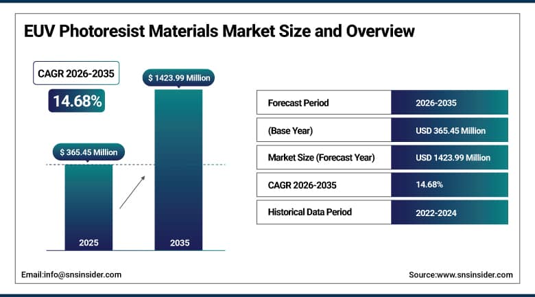
The EUV Photoresist Materials Market size was valued at USD 365.45 million in 2025 and is expected to reach USD 1423.99 million by 2035, growing at a CAGR of 14.68% from 2026-2035.
The EUV Photoresist Materials Market is witnessing strong growth due to the rising application of extreme ultraviolet lithography technology in advanced semiconductors and increasing needs for small, compact, and efficient electronic devices. The shift towards advanced nodes is resulting in an increasing demand for photoresists having high performance and excellent resolution ability. Increasing production of semiconductors, growing applications in artificial intelligence, high-performance computing, 5G, and advanced memories are further fueling the market demand. Moreover, consistent investments in fabrication plants of semiconductors and technological developments in extreme ultraviolet lithography along with research on high sensitivity and defect-free photoresists are contributing to market growth.
In 2025, TSMC reported that 7-nm and more advanced technologies accounted for 74% of total wafer revenue, up from 69% in 2024, highlighting the growing production of advanced semiconductor nodes and demand for EUV lithography.
To Get More Information On EUV Photoresist Materials Market - Request Free Sample Report
EUV Photoresist Materials Market Trends
-
Rising adoption of extreme ultraviolet lithography for advanced semiconductor nodes is driving demand for high-performance EUV photoresist materials globally.
-
Increasing production of 3 nm, 5 nm, and next-generation semiconductor chips is accelerating demand for advanced photoresist formulations.
-
Growing investments in semiconductor fabrication facilities are expanding opportunities for EUV photoresist materials across leading-edge manufacturing applications.
-
Advancements in metal oxide and chemically amplified resist technologies are improving resolution, sensitivity, pattern fidelity, and process performance.
-
Increasing demand for artificial intelligence, high-performance computing, and advanced data centers is supporting semiconductor manufacturing and EUV photoresist adoption.
U.S. EUV Photoresist Materials Market Size Outlook
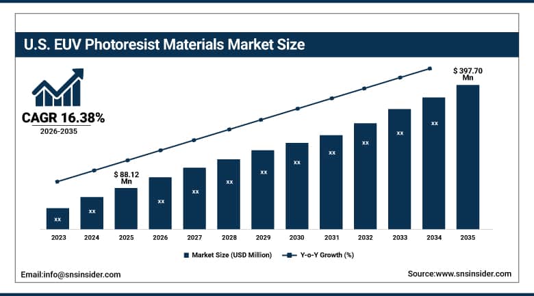
The U.S. EUV Photoresist Materials Market was valued at USD 88.12 million in 2025 and is expected to reach USD 397.70 million by 2035, growing at a CAGR of 16.38% from 2026-2035.
The U.S. EUV Photoresist Materials Market is experiencing strong growth due to rising investments in semiconductor manufacturing using advanced technology and an increased use of extreme ultraviolet lithography technology in advanced process nodes. With rising production of advanced semiconductors that are being used for artificial intelligence, high-performance computing, data center, and advanced consumer electronic products, the demand for high-performance EUV photoresist material is rising. Furthermore, the rising manufacturing capability of domestic semiconductor manufacturers due to the initiatives taken by the government along with investments in advanced fabs is adding up to the market demand.
TSMC announced plans to increase its planned investment in the U.S. to $165 billion, including additional fabs and advanced packaging facilities in Arizona. The expansion is aimed at supporting AI and advanced computing demand.
EUV Photoresist Materials Market Segment Analysis
-
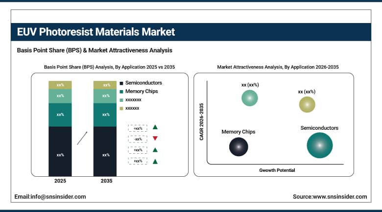
By Application, Semiconductors dominated the EUV Photoresist Materials Market with 38% share in 2025; Memory Chips is expected to grow at the fastest CAGR of 16.94% from 2026–2035.
-
By Resist Type, Chemically Amplified Resists (CAR) dominated the EUV Photoresist Materials Market with 74% share in 2025; Metal Oxide Resists (MOR) is expected to grow at the fastest CAGR of 16.60% from 2026–2035.
-
By Node Compatibility, Advanced Nodes (5 nm–7 nm) dominated the EUV Photoresist Materials Market with 57% share in 2025; Leading Edge (3 nm and Below) is expected to grow at the fastest CAGR of 15.24% from 2026–2035.
-
By End User, Consumer Electronics dominated the EUV Photoresist Materials Market with 37% share in 2025; Automotive is expected to grow at the fastest CAGR of 16.64% from 2026–2035.
By Application, Semiconductors dominate the euv photoresist materials market, Memory Chips grow fastest.
Semiconductors segment dominated the EUV Photoresist Materials Market with the highest revenue share of about 38% in 2025 because of extensive use of EUV lithography in cutting-edge semiconductor manufacturing. With an increase in requirements of small process nodes, higher densities of transistors, and better chip performance in particular, especially in applications of AI, data centers, smartphones, and high-performance computers, EUV photoresist usage remained significant.
Memory Chips segment is expected to grow at the fastest CAGR of 16.94% from 2026-2035 Propelled by growing demand for high-performance memory chips used in artificial intelligence, cloud computing, data centers, smartphones, and other electronic products. Growth of advanced DRAMs and NAND production, use of EUV lithography in future generation memory chip production processes, and fabrication facility investments should lead to higher growth in this segment.
By Resist Type, Chemically Amplified Resists (CAR) dominate the euv photoresist materials market, Metal Oxide Resists (MOR) grow fastest.
Chemically Amplified Resists (CAR) segment dominated the EUV Photoresist Materials Market with the highest revenue share of about 74% in 2025 due to its known compatibility with extreme ultraviolet lithography, high sensitivity, good resolution, and great commercial readiness. The widespread use by top semiconductor producers, reliable process integration, and ongoing enhancements to patterning capabilities have reinforced the position of CAR in advanced semiconductor manufacturing.
Metal Oxide Resists (MOR) segment is expected to grow at the fastest CAGR of 16.60% from 2026-2035 due to its better EUV absorption properties, higher resolution, enhanced pattern fidelity, and possibility of minimizing random defects. Rising needs for lithography at the sub-nanometer nodes, along with the research and development of metal-based resist material, is set to propel the adoption of this technology among semiconductor manufacturers.
By Node Compatibility, Advanced Nodes (5 nm–7 nm) dominate the euv photoresist materials market, Leading Edge (3 nm and Below) grows fastest.
Advanced Nodes (5 nm–7 nm) segment dominated the EUV Photoresist Materials Market with the highest revenue share of about 57% in 2025 due to EUV lithography technology being more extensively adopted in high-volume production at these proven advanced nodes. High production of CPUs, memory components, and fast chips, alongside developments in advanced fab facilities, ensured the demand for EUV resists was high.
Leading Edge (3 nm and Below) segment is expected to grow at the fastest CAGR of 15.24% from 2026-2035 owing to rising demand for higher densities of transistors, greater power efficiency, and better computing capability. Increased manufacture of AI chips, high-performance chips, and advanced mobile chips, along with greater investment in next-generation fabs, is likely to boost the uptake of EUV photoresists.
By End User, Consumer Electronics dominates the euv photoresist materials market, Automotive grows fastest.
Consumer Electronics segment dominated the EUV Photoresist Materials Market with the highest revenue share of about 37% in 2025 owing to the high demand for semiconductors, memory chips, and miniaturized semiconductor components for use in smartphones, laptops, tablets, and other internet of things devices. The increasing consumer demand for better performance, energy efficiency, and electronic features kept pushing the need for semiconductor production and EUV photoresists..
Automotive segment is expected to grow at the fastest CAGR of 16.64% from 2026-2035 As a result of rapid electrification, the growing use of ADAS, autonomous technology, and connected vehicles. The rising demand for automotive semiconductors, power management solutions, sensors, and computing chips, along with the increase in semiconductor content per car, will drive the demand for EUV photoresist materials.
Regional Analysis
|
Region |
Major Country |
Share within Region, 2025 (%) |
|---|---|---|
|
North America |
United States |
88.0% |
|
Europe |
Germany |
27.5% |
|
Asia Pacific |
China |
24.8% |
|
Middle East & Africa |
UAE |
23.0% |
|
Latin America |
Brazil |
39.5% |
Asia Pacific EUV Photoresist Materials Market Insights
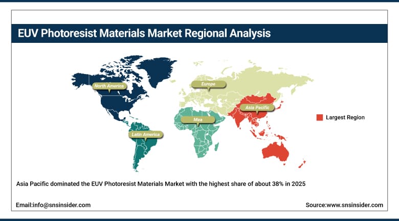
Asia Pacific dominated the EUV Photoresist Materials Market with the highest share of about 38% in 2025, The demand is driven by the presence of a robust semiconductor manufacturing industry in the region, especially in China, Taiwan, South Korea, and Japan. Increased capital expenditure on semiconductor production and the increased usage of EUV lithography in advanced node production are fueling the regional demand.
The China EUV Photoresist Materials Market accounted for a market share of 24.8%, supported by the rapid expansion of semiconductor manufacturing, increasing investments in advanced chip fabrication facilities, and growing demand for high-performance materials. Semiconductor manufacturers are strengthening production capabilities to meet rising requirements from AI, consumer electronics, automotive electronics, and high-performance computing. Government support for semiconductor self-sufficiency, expanding research and development activities, technological advancements, and increasing investments in domestic chip manufacturing are further encouraging the adoption of EUV photoresist materials across China.
Get Customized Report as Per Your Business Requirement - Enquiry Now
North America EUV Photoresist Materials Market Insights
North America is expected to grow at the fastest CAGR of about 15.93% from 2026 to 2035, backed up by the increasing investment in domestic semiconductor chip production, expansion in advanced fabrication plants, and increasing need for AI, high-performance computing, and data center chips. The additional factors behind the increased demand for photoresists are the incentives provided by governments, development of new technology, and adoption of EUV lithography.
The U.S. EUV Photoresist Materials Market accounted for a market share of 88.0%, supported by rising investments in advanced semiconductor manufacturing and growing demand for high-performance materials used in next-generation chip production. Semiconductor manufacturers are expanding advanced fabrication capabilities to support applications in AI, high-performance computing, and data centers. Strong government support for domestic semiconductor production, ongoing research and development, technological advancements, and increasing demand for smaller and more powerful chips are further driving the adoption of EUV photoresist materials across the country.
Europe EUV Photoresist Materials Market Insights
Europe EUV Photoresist Materials Market is witnessing steady growth, Backed by advancements in semiconductor research, advances in lithography technology, and growing investment in local chip fabrication capacity. The countries making the biggest contributions include Germany, Netherlands, Belgium, and France, which have robust semiconductor ecosystems and world-class research facilities. Advancements in next-generation EUV and High-NA EUV technology, increasing need for advanced node chips, and measures under the European Chips Act are driving up regional demand for high-quality photoresists.
Germany EUV Photoresist Materials Market accounted for a market share of 27.5%, supported by strong investments in advanced semiconductor manufacturing and growing demand for high-performance materials used in next-generation chip production. Semiconductor manufacturers are expanding fabrication capabilities to meet the rising demand for advanced chips used in AI, high-performance computing, automotive electronics, and consumer devices. Germany’s established semiconductor industry, focus on technological innovation, strong research capabilities, and increasing investments in domestic chip manufacturing are further supporting the adoption of EUV photoresist materials across the country.
Middle East & Africa and Latin America EUV Photoresist Materials Market Insights
Middle East and Africa, and Latin America EUV Photoresist Materials Market is showing slow growth because of the rise in semiconductor investments, growing electronics manufacturing, and the growing requirement of advanced chips. Government initiatives towards technology localization, semiconductors, and digital infrastructure are contributing to future prospects. But at present, there are less advanced wafer fab infrastructure and technological infrastructure as compared to the other semiconductor manufacturing regions.
The UAE EUV Photoresist Materials Market accounted for a market share of 23.0%, supported by growing investments in advanced semiconductor technologies and increasing efforts to strengthen high-tech manufacturing capabilities. Rising demand for advanced chips across AI, telecommunications, automotive electronics, and consumer devices is creating new opportunities for high-performance photoresist materials. Government initiatives promoting technology development, industrial diversification, semiconductor-related investments, and expanding research activities are further supporting market growth and increasing the adoption of EUV photoresist materials in the UAE.
Market Dynamics
Growth Drivers: Rising semiconductor investments for AI and high-performance computing are strengthening demand for advanced EUV lithography materials
Rapid growth in artificial intelligence, high-performance computing, cloud infrastructure, and advanced electronics is increasing demand for sophisticated semiconductor chips manufactured using leading-edge lithography. The EUV technology helps semiconductor manufacturers create increasingly intricate ICs with reduced feature sizes. With chipmakers ramping up their capacities for AI accelerators, processors, advanced memory chips, and network components, the demand for photoresist materials for the EUV technology keeps rising. Initiatives by the government aimed at boosting domestic semiconductor manufacturing and huge capital investments by top-tier foundries keep the market potential high. Competition among semiconductor manufacturers for reducing process nodes is another factor stimulating the adoption of more sophisticated lithography technology solutions, driving the demand for EUV photoresist materials.
Restraints: High development complexity and stringent performance requirements increase production challenges for EUV photoresist manufacturers
The complex development and manufacturing requirements associated with EUV photoresist materials represent a significant market challenge. EUV lithography requires very short wavelengths, which means that the photoresists have to be designed to provide outstanding resolution, sensitivity, line edge roughness, and defectivity. The formulation of such photoresists that provide the above parameters is complex and includes sophisticated chemistry, testing, high purity of raw materials, and tight control of contamination. Minor differences in the chemical composition of photoresists can greatly influence the efficiency of the manufacturing process and pattern quality. Consequently, advanced facilities for research and long qualification procedures are needed by the manufacturers before any market introduction of the photoresist.
Opportunities: Expanding semiconductor fabrication capacity creates significant opportunities for advanced EUV photoresist material suppliers worldwide
Increasing investments in semiconductor fabrication facilities are creating significant opportunities for EUV photoresist material manufacturers. The semiconductor industry is increasing its advanced node production capabilities due to the rising need for AI processors, HPC, advanced smartphones, automotive chips, and many more complex electronics. The development and expansion of fabrication facilities require lithography materials that can keep up with increasing complexities in pattern generation processes. In addition, government programs and efforts geared towards improving the semiconductor supply chain within the country are helping build new fabrication facilities in key semiconductor manufacturing areas. With the increasing use of EUV lithography in advanced nodes, the demand for high-performance photoresists is expected to rise. Those who will be able to develop better formulas will benefit from this trend.
Recent Developments:
-
2026: TOK is developing next-generation EUV photoresists spanning chemically amplified, metal oxide, and small-molecule resist technologies to address further semiconductor miniaturization requirements.
-
2026: DuPont highlighted its Eon™ EUV resist platform, designed to provide higher resolution, improved line-width roughness, stronger critical-dimension uniformity, and faster photospeed for EUV and high-NA EUV.
-
2025: JSR and Lam Research entered a cross-licensing and collaboration agreement to accelerate next-generation patterning, including dry-resist technology for EUV lithography and advanced semiconductor materials
-
2025: Fujifilm showcased its latest EUV resist and EUV developer research at SPIE 2025, highlighting advanced lithography materials designed to support high-resolution semiconductor patterning.
EUV Photoresist Materials Companies are:
-
Tokyo Ohka Kogyo Co., Ltd. (TOK)
-
Fujifilm Holdings Corporation
-
Shin-Etsu Chemical Co., Ltd.
-
Brewer Science, Inc.
-
Inpria Corporation (JSR)
-
Merck KGaA (AZ Electronic Materials)
-
DuPont de Nemours, Inc.
-
Dongjin Semichem Co., Ltd.
-
Avantama AG
-
Lam Research Corporation
-
LG Chem Ltd.
-
Arkema S.A.
-
Tokyo Electron Limited
-
S&S Tech Corporation
-
Kayaku Advanced Materials, Inc.
-
GlobalWafers Co., Ltd.
-
Integrated Micro Materials LLC
-
Irresistible Materials Ltd.
EUV Photoresist Materials Market Report Scope:
| Report Attributes | Details |
|---|---|
| Market Size in 2025 | USD 365.45 Million |
| Market Size by 2035 | USD 1423.99 Million |
| CAGR | CAGR of 14.68% From 2026 to 2035 |
| Base Year | 2025 |
| Forecast Period | 2026-2035 |
| Historical Data | 2022-2024 |
| Report Scope & Coverage | Market Size, Segments Analysis, Competitive Landscape, Regional Analysis, DROC & SWOT Analysis, Forecast Outlook |
| Key Segments | • By Resist Type (Chemically Amplified Resists (CAR), Metal Oxide Resists (MOR), Non-Chemically Amplified / Dry Resists) • By Node Compatibility (Leading Edge (3 nm and Below), Advanced Nodes (5 nm–7 nm), Other Nodes) • By Application (Semiconductors, Integrated Circuits, Microprocessors, Memory Chips, Other Applications) • By End User (Consumer Electronics, Automotive, Telecommunications, Healthcare, Other End Users) |
| Regional Analysis/Coverage | North America (US, Canada), Europe (Germany, UK, France, Italy, Spain, Russia, Poland, Rest of Europe), Asia Pacific (China, India, Japan, South Korea, Australia, ASEAN Countries, Rest of Asia Pacific), Middle East & Africa (UAE, Saudi Arabia, Qatar, South Africa, Rest of Middle East & Africa), Latin America (Brazil, Argentina, Mexico, Colombia, Rest of Latin America). |
| Company Profiles | JSR Corporation, Tokyo Ohka Kogyo Co., Ltd. (TOK), Fujifilm Holdings Corporation, Shin-Etsu Chemical Co., Ltd., Brewer Science, Inc., Inpria Corporation (JSR), Merck KGaA (AZ Electronic Materials), DuPont de Nemours, Inc., Sumitomo Chemical Co., Ltd., Dongjin Semichem Co., Ltd., Avantama AG, Lam Research Corporation, LG Chem Ltd., Arkema S.A., Tokyo Electron Limited, S&S Tech Corporation, Kayaku Advanced Materials, Inc., GlobalWafers Co., Ltd., Integrated Micro Materials LLC, and Irresistible Materials Ltd. |
Frequently Asked Questions
The EUV Photoresist Materials Market is expected to grow at a CAGR of 14.68%from 2026 to 2035.
The EUV Photoresist Materials Market was valued at USD 365.45 million in 2025.
The major growth factor driving the EUV Photoresist Materials Market is the increasing adoption of advanced semiconductor nodes, including 5nm, 3nm, and below, requiring high-performance EUV photoresists for precise, high-resolution chip manufacturing.
The Chemically Amplified Resists (CAR)segment dominated the EUV Photoresist Materials Market in 2025.
Asia Pacific dominated the EUV Photoresist Materials Market in 2025.
